| MediaWiki:Sitenotice |
|---|
| 2026-03-12: Cocopedia.com is now using a new caching system that should make things faster. Please let me know if you encounter any new issues.
2026-03-15: MediaWiki has been reinstalled and the old database and files restored. It was pretty clogged up from being upgraded so many times since 2004. I am also testing out Cloudflare to see if it can prevent the 'bot assaults that took the site down last year. 2026-03-16: Special thanks to Don Barber for hosting a backup mirror of CoCopedia: https://cocopedia.dgb3.net |
User:Computerdoc
| WELCOME |
|---|
| Looking for CoCo help? If you are trying to do something with your old Color Computer, read this quick reference. Want to contribute to this wiki? Be sure to read this first. This CoCo wiki project was started on October 29, 2004. --OS-9 Al Read-only mirror: https://cocopedia.dgb3.net |
See Recent Changes. | About this site. | Join the E-Mail List or Facebook Group. | Contact me with updates/questions.
This page was last updated on 08/19/2024. Total Pages: 751. Total Files: 999.
Home / User List - Computerdoc
Introduction
- First and foremost, I would like to express my gratitude and appreciation to Allen Huffman for extending an invitation to me to host my personal web page on his Cocopedia web server.
- I invite you to check back periodically as I document my experiments with my Coco 3 setup and my 6809/6309 microprocessor computer projects.
Computer Repair Service Available in Manning, SC
- First, the business aspects of my life.
- I'm a Computer Consultant by trade and offer Computer Repair Services, PCB building, Network Services in the Southeastern area of South Carolina. You can contact me with your specific needs at my email address by referring to the Contact section of this web page.
EPROM Burning Service Available
- I am now setup to burn many different devices including Color Computer compatible 8K x 8 and 16K x 8 EPROMs. I also can burn many other sizes as well. Please email me with specific details and requirements.
Contact Information
- You can email me at
c o m p u t e r d o c at s c dot r r dot c o m
for further information. Just remove the spaces and replace the words 'at' and 'dot' with the appropriate punctuation marks to arrive at a usable email address. The weird spacing and words is to try to prevent bots from automatically getting my email address of course.
- I can also be found on the Coco List. To subscribe go to http://five.pairlist.net/mailman/listinfo/coco for further information.
- I'm also on Skype as
d r w h o 7 7 7 7
and also on Yahoo Messenger as
d r w h o 7 7 7 7
and of course you can call me on the phone. If you wish to call me, please send me an email requesting the needed information.
- Thank you.
- Now that the business part of my life is out of the way, LET'S HAVE SOME FUN!
Taking Off Into A Different Direction!
September 16, 2016
- For a while now I have been working in a slightly different Direction. I have been wanting to build a 68000 based computer ever since I was able to grab some 68000 and 68HC000 64 pin DIP chips. I scoured the internet like I did several years back looking for 6809 projects. I finally came across a project build by a gentlemen named Roger Hanson. He breadboarded a 68000 microcomputer and eventually fabricated a PCB with 2MBs of static ram, 64KB of Eprom, 2 Serial ports, 4 - 8-bit parallel ports with a 5th parallel port on the 68681 DUART (Dual Universal Asynchronous Receiver Transmitter) chip. This is the 1st 68K Board I ever built and it worked the first time!
Building a 68000 Single Board Computer
- This section is under construction as I am writing this while I am in the middle of building an IDE version of the 68K Board the details of which are in the next section. I'm kind of writing this in reverse so please bare with me.
68K SBC
- This is where I will describe my very 1st 68000 board I have ever built. To whet your appetite, here is a picture of the board powered up. Stay tuned.

- A full description of this board will be forthcoming. Yes, I can download and run a forth interpretor on this board even without an IDE Interface or Disk Operating System! I have also run a Tiny BASIC Interpreter on this board. The 3KB TBI program is quite dwarfed by the 2MBs of Static Ram. :)
- MORE TO COME!!!
Adding An IDE Interface to the 68000 SBC Version 2
September 16, 2016
- I am very excited about this next version of the platform. This version has all the features of the 1st version of the 68K board plus the addition of an IDE Interface port that will support a CF to IDE Adapter Card. So far only CF adapter cards have been used, but I imagine a real hard disk drive will work as well. May be even an SD to IDE Adapter Card the last of which I will hopefully be testing at some point. I have to build this board 1st!
- As always I gathered up all the resistors and capacitors needed by this board, installed and soldered them onto the 2nd version of this 68K Board.
- Next, I soldered machined female headers for sockets which saves quite a bit in the funds department. :)
- Once all the sockets were installed, I went through the rest of my parts and ICs to see what parts I have on hand before I put in an order to Digikey. I was able to find quite a bit actually. I am holding off installing the 68HC000 16MHZ chip and the 2 - 4Mbit, 512KB Flash Memory chips until after everything else on the 68K Board is complete. A picture of the IDE Version of this 68K Board is at the following url. My 68K Board with IDE after installing all the parts I have on hand This picture shows the 68K Board with all the parts I have on hand soldered into place. After double and triple checking the parts list I have entered at Digikey, I will be submitting the order for the rest of the parts needed to complete this board.
- The rest of the build description is forthcoming.
- This is a picture of the finished 68K SBC V2 board.

- Here is the 2nd board powered up and running.

- I'm currently running the 2nd board at 8MHZ, but I will be ordering 12MHZ and 16MHZ oscillators soon. I want to see how fast this board will run. The 68000 CPU part number is MC68000P12F and and the 2nd line is a marking of 16MHZ on the chip itself. I wonder if the 68000 will run reliably at 16MHZ. Inquiring minds want to know! Once I get my 2nd 68K board running at the fastest reliable speed, then I will work on upgrading the speed of my 1st board.
My Altair 8800!
July 15, 2015
- Yes, Yes. I know this is a 6809 Color Computer page, but since I have Multicomp PCBs run 6809 and Z80 microprocessor based microcomputers, I thought I might as well add this to the mix. I have been looking over some Altair web sites recently and I'm thinking about restoring my original Altair 8800! The following dropbox link has all the pictures I took of this baby a few years ago. Pictures of My Altair 8800 Inside and Out I didn't want to cludder up my nice CoCo page! :) I'm thinking of branching off this Altair section to another page though. If that happens, this portion will go there.
- In the way of restoration, not much has happened as of yet. I have been doing a lot of studying on the boards that are in my Altair 8800 to determine exactly what they are. This is what I have come up with so far according to the pictures and explanations on the S-100 Computers' web page at S-100 Computers. This web site has been a big help in this endeavor as they have pictures of many S-100 boards along with explanations of what they are.
These are the boards I have so far as I can determine from what little experience I have with Altair microcomputers.
- MITS 8800 D/C BD REV. 1 Front Panel
- MITS 8800 CPU BD REV. I 8080A CPU Board
- The ZPU Board 1976 by Technical Design Labs REV. I 1977
- IMSAI 4K Static Ram Board
- MITS 88-4KD Early 4K Dynamic RAM Board - S-100 Computers.com says to not use it!
- RAM 4 REV. I 1975 unknown make
- ALS-8 8K PROM 34 Processor Technology
- MITS 88-SIOB Serial TTL REV. 1 I/O board
- MITS 88-4PIO REV. O 4 port Parallel I/O Board
- 88-ACR Cassette Interface Board
- A Processor Technology VDM-1 Composite Video Board 1976
- A Godbout Bus Terminator Board
- IMASI PIC-8 REV. 3 IMS Asscociates Inc. 1975
- MITS Modem Board
- A few IMSAI boards as well. Can they co-exist in an Altair with the Altair boards?
- A few small boards of unknown purpose that look like they are missing some power transistors of some type.
- Some of these boards have chips missing as well.
- What I don't have is any kind of online storage such as floppy drive controllers or hard drive controllers and drives which at the very least I must have in order to make use of the software I found. To alleviate the storage problem as inexpensively as possible, I have been considering building Josh Bensadon's 8080A Altair / IMSAI CPU Board which is loaded with features not the least of which is an SD Card Interface using discrete components and no microcontroller was used to interface it! Josh himself told me about his creation so I looked it up. It is quite a board. It will have to be a slow build though.
- Here are the features that I remember reading about. It has 64KB of ram, 4 serial ports, 2 parallel ports, both Altair and IMSAI front panel connectors, an SD Card Interface for online storage, buffering to the S-100 bus, and the ability to disable any function of the CPU board including the 8080A CPU itself so it can co-exist with other boards in the computer as well as become a slave board instead of the master. I can't wait for the current version to be release later on this month by Josh.
- In the meantime, I'm going to start examining the power supply first. I have a dilemma though. This Altair is so early in the production at MITS that the front panel is soldered to the backplane as is the wires from the power supply. Even after I ensure nothing in the power supply is shorted out due to age, I still cannot do a smoke test until I know for sure that the voltages are in spec. I'm still thinking how I'm going to accomplish that.
- If anyone out there in Altair Land has restored an Altair that is willing to guide me through this restoration, please get in contact with me. I'm on the Altair Computer Club email list as well as on the N8VEM email list.
My Adventures with Eagle - The Schematic Entry and PCB Design Program
July 13, 2013
- Although it has been quite awhile since I have updated this web page, I have been very busy learning how to design and have fabricated printed circuit boards (PCBs). At first I chose KiCAD for this purpose and although it is a very interesting program for this purpose, I did not like the fact that autorouting was not built in to the program. After placing the parts on the PCB layout, the user has to go to an external web page to do the autorouting. After asking around on the Coco List and a longtime best friend, I have decided to change to Eagle and learn it instead. I have been practicing entering schematics for a number of projects which I will eventually talk about here on this web page, but suffice it to say that I have gained a basic understanding of how Eagle works. I now understand why so many people on the Coco List and elsewhere on the internet are so keen on using this fine software package.
- At this point I'm using the free version of Eagle so all my projects will have to fit on a PCB about 4" x 4" in size.
- All my projects will use through hole ICs to make it easier for people new to soldering to assemble the project kits.
- In the beginning the projects were very small and as I gained experience with Eagle, they grew in size. The first projects I played with were projects other people had created like:
- A Slot Extender for the Color Computer - I actually had this one made.
- A Simple 8-Bit Video Graphics Card with 64KB of static ram and a CPLD for all the logic.
- A 512KB Ram Card using two 30-pin SIMM memory modules with 256 cycle refresh
- A Multi-DOS Pak using a 1MB memory chip fully addressable using software
- An 8 Slot Multi-Pak Interface
- A Megavore that uses an Atmel XMega chip
- A PS/2 Mouse Interface
which if you ask me is a nice list of projects to start learning from. As I gained experience, I started playing with a few very small projects like:
- A DB9 RS-232 Connector to Pin Header Adapter suitable for breadboarding
- A 40-Pin Header to Coco Slot Receptical Adapter - mates with the Slot Extender above to allow any Coco Cartridge Pak to connect to the Color Computer's internal slot so the entire PCB can be seen and tested. I plan to use this during all the testing of my Coco Slot compatible projects.
- An IDC 40-Pin Connector to 40 Pin Breadboard Adapter - I'll be using this one to connect my breadboarded prototyped projects to the Coco to make sure the circuit works before having a PCB fabricated.
- A Color Composite Video Output Interface - an implementation of Marty Goodman's Composite Video Monitor Circuit.
just to name a few. I have started several projects for the Coco which will remain a mystery for now until they are completed.
Implementing Grant Searle's 6-Chip 6809 Single Board Computer (SBC), 32KB Ram, Serial I/O at $A000
- Now I have finally gained enough experience to seriously consider entering the schematic for Grant Searle's 6-Chip 6809 Computer and design a PCB to turn my prototype into a real 68B09 single board computer with 32KBs of ram and a serial port at $A000. I have added a few minor modifications to the original design. I included RESET and HALT pushbuttons as well as LEDs for RESET and HALT for easy start and restart of the computer. I also added two more LEDs for the BA and BS outputs of the 6809 to more easily tell what the 6809 processor is doing.
- Then I created several variations of Grant's 6-chip computer.
Grant Searle's 6-Chip 6809 Single Board Computer (SBC), 40KB Ram, Serial I/O at $A000
- The first obvious change was adding more memory to the basic project. There is a hole in the memory map from $8000 to $9FFF which is between the current ram in the system and the serial port at $A000, so I designed my first real computer circuit add-on by adding 8KBs of ram using a 32KB static ram chip. This was pretty simple for me as I had been reading a bunch of IC Datasheets by this time.
Grant Searle's 6-Chip 6809 Single Board Computer (SBC), 48KB Ram, Serial I/O at $D000
- The next update was to move the Serial I/O port from $A000 to $D000. Since the Basic code starts at $DB00, this was as high as I wished to go up to now. Then I added 8KBs more of ram to the system to raise the total ram up to 48KB of contiguous memory for the 6809 Extended Basic Interpreter in this cool little project. Since the 27128 Eprom starts at $C000 I'll have to devise a circuit to prevent the ram from being accessed when the serial I/O port or the eprom is being accessed which won't be hard. Just a little logic and it will be good to go.
Grant Searle's 6-Chip 6809 Single Board Computer (SBC), 55.5KBKB Ram, Serial I/O at $FF00
- Next I wanted to make this computer compatible with the Coco, so to begin with I raised the Serial I/O port to $FF00 and opened up $FF00 to $FFEF for I/O and prevented the Eprom from being accessed.
Grant Searle's 6-Chip 6809 Single Board Computer (SBC), 56KB Ram, Serial I/O at $E000
- It was suggested by some friends on the Coco List to run Flex9 on this little gem, so I changed the serial I/O port to $E000 so as to be compatible with Flex9.
- At this point I rested my brain for a little bit and thought about all I had done with my little computer.
Coco 1 & 2 Color Composite/Component Video Monitor Driver with Sound
- As you might have noticed below in the Coco Sections, I have not included a Coco 2 in my Computer Data Center yet. The reason is none of my Coco 2s have a Composite Video Monitor Driver board in them. Wanting to be able to run a Coco 2 in my Color Computer Data Center I decided to build me a PCB to do just that, give my Coco 2 a composite video output.
- After much searching and having found several versions of several solutions, I finally picked Marty H. Goodman's Color Monitor Driver design and decided to build it. When I was entering this design into Eagle, I remembered some other designs that I had downloaded off the internet for a Component Video Design, a design with a Color Composite output and a Monochrome driver output along with a sound output. I decided to make a combined version that turned out quite well if I do say do myself. It has three video amplifiers using Marty's design so the user can hook up to the MC1372 chip inside the RF CAN to obtain a Color Composite feed as well as a Luminance, Cr and Cb feeds for Component Video. A mono sound circuit is also included.
- I sent the PCB design to be fabricated and when the three prototype PCBs have been completed and I have received them I will populate one of the boards soon and post a video of this board in action to YouTube and send a link to it to the Coco List. I will also include the link here. I'll keep you posted with continuing updates for this project.
My Korean Coco 2B Internal Eprom Adapter
- I have been working on a PCB design to get HDB-DOS running internally inside a Korean Coco 2B. When I receive the PCBs back from the fabricators, I'll populate one of the PCBs and install it into my Korean Coco 2B. Why the Korean Coco 2B you ask. Well I'm glad you asked that question.
- A while back a member of the Coco list mentioned that he was booting Extended Color Basic from cassette. He asked for an Eprom to be burnt with CB 1.3 and ECB 1.1 for him. I asked him would he like anything else added to his Coco. He asked me if I had any ideas. Well, actually I did have one, so I said yes. Would he like to be able to boot straight into HDB-DOS without any cartridge. He said yes he would, so I put together an Eprom image with Color Basic(CB) 1.3, Extended Color Basic(ECB) 1.1 and HDB-DOS 1.3 with Drivewire 3 for a Coco 2, burnt all this into a 27256 Eprom and sent it to him. I emailed him the installation instructions thinking I had covered all the bases. Since I had gained so much help from others on the Coco List, I was excited to be able to finally help someone else.
- In designing and typing up the instructions for the eprom installation, I had overlooked something. Some of you may have already figured this out. I had not considered the !CTS signal needed by the HDB-DOS part of the Eprom in order to run correctly which was made painfully obvious to me when I received an email stating that the Coco 2B did not boot even though the A14 address line pin 27 of the Eprom was tied to A14 pin 22 of the 6809 CPU. When they disconnected the A14 line on pin 27 and installed the Eprom with all the pins inserted into the socket where the original 27128 Eprom had been, that did not work either.
- Well, I immediately started researching the cause of this dilemma and realized I had not included the !CTS Cartridge ROM signal in with the Chip Enable signal of the socket. Plugging the 27256 Eprom straight into the socket didn't work either because the A14 signal on pin 27 of the 27256 was a !PGM signal on the 27128 which was connected to 5V! The A14 address line pin 27 needs to be connected to ground to boot into Extended Color Basic 1.1. Knowing I would need to include another IC into the mix, I decided to design a PCB that would make running HDB-DOS in the same Eprom as CB 1.3 and ECB 1.1 possible. I think I have come up with a design that will do just that.
- I am waiting for the PCBs to arrive so I can test out my design. Hopefully I have done my homework correctly and I will have a Korean Coco 2B running HDB-DOS without a cartridge. Thinking on the possibilities of such a setup, I would be able to use just a serial cable and connect up to a Drivewire 4 Server running on a PC without any external cartridges. Why is this so cool? I'd be able to reduce the amount of hardware I would need if I ever needed to carry my Coco to a meeting. All I would need is the Coco 2B, the serial cable, the monitor and a laptop running Drivewire 4. No cartridges nor multipaks would be necessary! This would reduce the amount of needed equipment to carry to a color computer club meeting or a Coco convention should someone wish to demonstrate his latest version of a Coco game or most recent version of the latest and greatest NitrOS-9 utility. Now That Is Cool! I'll keep you guys posted with continuing updates as they happen on this exciting project.
October 24, 2013
- After waiting for back ordered parts to arrive from Newark and long waits for some more parts to arrive from China, I have finally fully assembled the Internal HDB-DOS Eprom Upgrade PCB for its first test. I hooked it up with the 27256 16KB Eprom installed with the Color Basic 1.3, Extended Basic 1.1 and the HDB-DOS DW3 Coco 2 machine code programmed within. I powered up the Coco 2B and I got ... Zip, Nada, Nothing! All I saw was the now all too familiar orange bands and green @ signs bands on the screen, so I knew the video circuitry was functional. The MC6809EP microprocessor did not boot which means something is wrong with the MPU reading the machine code out of the eprom.
- I thought for a bit and decided to use the Color Basic 1.3 & Extended Basic 1.1 machine code which resides in the original 27128 eprom in the next test that I had taken out of the Korean Coco 2B in order to conduct this first test. I figured since this code is proven functional, I can eliminate the possibility of an incorrectly programmed eprom from the mix of things happening or more appropriately not happening in the first test.
- So I pulled both ICs out of the PCB and installed a jumper in the 14 pin socket to allow the chip select signal to pass through the 14 pin socket to the 27128 Eprom IC. Then I connected the blue A14 wire to +5V since on the 27128 eprom pin 27 is the programming pin which uses active low logic. This keeps the eprom out of the programming mode. The orange Cartridge Select wire is not connected to anything since I’m not testing HDB-DOS yet. In this configuration the Korean Coco 2B booted up and I was greeted with the familiar
EXTENDED COLOR BASIC 1.1
COPYRIGHT © 1982 BY TANDY
UNDER LICENSE FROM MICROSOFT
boot message! Success has finally been achieved! A basic test of the functionality of most of the PCB is complete. Now I need to program this same code into a 27256 chip and reconfigure the PCB so the 6809 MPU chip will correctly boot the ECB 1.1 machine code again. Once that is successful, then I can progress on towards including the HDB-DOS code into the upper portion of the 27256 eprom chip and reconfigure the PCB one more time.
- So, what have I accomplished so far? All the data lines (D0 – D7) and 13 of the address lines (A0 – A13) function correctly on the PCB as well as the original Chip select line which is just about the entire PCB. All that’s left to test basically is to reintroduce the Quad AND gate IC back into the mix and get it functioning. Here is a link to a photo showing the Internal HDB-DOS Eprom Upgrade PCB in its first successful test configuration. Yes the PCB does finally exist!

- It is beginning to look like a real Korean Coco 2B upgrade now. Notice the single hook clip on the wire! This upgrade will not need any soldering to install so just about everyone will be able to install it. That is my goal anyway. Keep on believing! It Will become a reality. More news coming as it happens!
512KB Memory Upgrade PCB for the Coco 3
March 1, 2014
- After a long absence from updating this page and having endured pneumonia for at least 6 weeks, I'm now ready to continue updating my Wiki page.
- I did a lot of research on 30-pin SIMMs to make sure I understood them correctly for sometime before I created and finalized the design and had the board made. Not fully understanding why PBJ had put a large Electrolytic Capacitor on their 512KB Memory Upgrade PCB I decided not to include it. Boy was I mistaken on that one, but more on that in a minute.
- After submitting my design to OSHPark.com for fabrication, I waited 10 days and received my brand new PCBs that I hoped to turn into an add-on for my Coco 3.
- I went to my workbench in my shop and began to populate the PCB. When I was finished building the PCB of which I actually built two of them I was ready to install one in my Coco 3 and check it out. This is what the board looks like.


- I had enough 0.1uf capacitors for the first PCB I made, but only 2 for the second PCB, so during testing I got some interesting results.
- The PCB with 4 capacitors booted NitrOS-9 6809 L2 v3.2.9 for the Coco 3 from floppy drive beautifully. I performed a few commands and then NitrOS-9 CRASHED! Well I pulled that PCB out of my Coco 3 and installed the PCB with just 2 capacitors. Well, guess what? It crashed quicker than the first one with 4 capacitors. I thought A-HA! I know what's going on. The PCB needs that larger electrolytic capacitor I saw on the PBJ 512KB Memory Upgrade PCB.
- I immediately ordered 25 - 100uf electrolytic capacitors since I planned on make more Coco 3 compatible PCBs of various types. When they came in I soldered one on each 512KB Memory Upgrade PCB across the +5V and GND pins of the pin headers. Now I went back to my test Coco 3 and installed the first PCB back in again and tested it one more time. This time NitrOS-9 booted successfully and ran all night and into the next day. I disassembled BASIC09 over and over to give the Coco 3 a long task to do. Then I would periodically list the BASIC09.ASM file I had created over and over to make sure the Coco 3 was still functional. It was all a fantastic success! I had made my first Coco 3 memory upgrade card and successfully tested it! I was ecstatic!
- I have now designed, built and tested a Coco 3 compatible 512KB Memory Upgrade Board as shown below installed in my test Coco 3.

- Here is a closer view of the PCB.

- Well, you are probably wondering something. Where is that 100uf electrolytic capacitor? I don't see it on the 512KB Memory Upgrade you built. I will say you have a good eye! All these pictures were taken before the 100uf capacitor was soldered on the PCBs. I was so excited about my success that I forgot to take new pictures of the updated version of the 512KB Memory Upgrade PCB. Since I had a customer in Quebec, Canada and North Carolina, USA I went ahead and mailed them not thinking no new pictures were taken. I'll have to take those pictures after I make another PCB. In the meantime, I now have an Internationally known business! I Love This Stuff!
- Take care my friends. Qaplah! StarFleet Out! End Transmission! :)
Coco Slot Extender with Eprom That Fits in a Game Cartridge
March 1, 2014
- I wanted to start experimenting with some cartridge pak circuits rolling around in my head that would plug into the Coco's Slot Receptical.
- To do that I took the Slot extender file for Eagle from the internet that's listed in several places and reorganized it so that it would fit inside an old game cartridge. I showed the design to a friend of mine in Australia and he said that was pretty cool! Actually he generously gave me the idea to repackage it inside a game cartridge to make it easy to prototype with, so I did.
- Next I got to thinking that since the slot extender would possibly be the only PCB plugged into the Coco slot receptical, the user would not be able to get to his files. My buddy in Australia gave me that idea too. I had been doing so many things designing this board and that board that I was having a difficult time coming up with ideas. I humbly that my buddy in Australia for all his help.
- I finally got the Coco Slot Extender with Eprom that fits inside a Game Cartridge Pak designed, so I submitted it to OSHPark.com for fabrication. I love these purple PCBs with gold contacts and pads everywhere. They are real pretty and professional looking. After I was done, my buddy in Australia wanted a bare board to save on cost, so off to the US Post Office and mailed him one. My second international customer! I'm really liking all this!
- Here is a few pictures of the completed Coco Slot Extender with Eprom.


- I did continuity checks on the entire PCB and everything was correct. Now I wanted to plug the Coco Slot Extender with Eprom into my Coco 3 and test the eprom portion of the PCB to make sure that a DOS ROM booted correctly. What better DOS ROM to test than HDB-DOS v1.4 DW3 for the Coco 3. I erased an eprom I had and burned an image of HDB-DOS v1.4 DW3 for the Coco 3 into the empty eprom and plugged it into the eprom socket. I then inserted the completed Coco Slot Extender with Eprom into my Coco 3 Slot Receptical and turned on the Coco 3. I am happy to report that I had my second success testing another one of my creations on my test Coco 3. HDB-DOS booted with flying colors and I was able to connect to Drivewire 4 Server on my PC and boot NitrOS-9 6809 L2 V3.2.9 Becker version for the Coco 3 from a .dsk file stored there. A true diskless Coco 3 with all the advantages of a total of 256 floppy and Hard drives combined into whatever order the user wishes.
- I have an additional idea to include with this PCB my buddy gave me that I'm going to develop, so stay tuned.
- Take care my friends and keep having fun with your Cocos! Qaplah! Starfleet Out! End Transmission! :)
Coco Hardware Development Adapter
June 6, 2014
- After having finished building several projects and getting them mailed, I finally finished my Coco Hardware Development Adapter! I'm at my favorite spot in a local Mickey D's updating this wiki page and I don't have my MicroSD to SD memory Card adapter with me, so I will have to add the pictures of the completed adapter after I get back home. In the meantime, here's the nitty gritty on the specifications of the Coco Hardware Development Adapter as I am calling this two PCB adapter.
- The adapter brings out all 40 contacts of the Coco's cartridge slot receptacle so it is compatible with All three Color computers, the Coco 1, 2 and 3. It enables the designer to interface any type of circuit the user wises to any of the Cocos utilizing any needed signals available on the Coco's expansion slot. This first version has NO BUFFERS included in the design so the user is responsible for ensuring that their circuit is compatible with the Coco prior to connecting the prototype circuit up to the Coco with this adapter.
- I will be designing a buffered version sometime in the near future, but just remember that this first version DIRECTLY CONNECTS to the COCO'S INTERNAL BUS!!! I will NOT BE RESPONSIBLE for any failures on any designers part for circuits incorrectly designed and connected to the Coco that end up messing up the user's Coco using this adapter!!!
- I will be including the pin out of the Coco's Slot with each adapter that is ordered. Sorry, I did not think to put the signal names on the smaller IDC to 40-pin Adapter PCB in this first version, but I'm thinking that I will add that to the next version.
- Hey, wait a minute. I just remembered that I do have a MicroSD adapter, so here are the first pictures of my Coco Hardware Development Adapter fully assembled.

- This is the top view of my Coco Hardware Development Adapter fully assembled.

- This is the bottom view of the Coco Hardware Development Adapter.
- I will be putting together a little demo of the adapter in use as soon as I get a chance to come up with the design of the demo circuit and get the needed buffer ICs ordered. Basically it will be a blinkenlights type of circuit showing all of the Coco's signals on a bunch of several different colored LEDs. I've got to either order a few more solderless breadboards or clear off a few I currently have in use.
- Until next time, Starfleet Out! Qaplah! End Transmission!
The Ultimate Eprom/Flash Pak for the Radio Shack Color Computers
September 8, 2014
- Recently I noticed a thread on the Coco Email List talking about taking .bin files <16KB in size that will fit in the $C000-$FEFF for the Coco 1 & 2 and $C000-$FDFF for the Coco 3 and adding a 33 byte program in from of it to place it in the correct area of ram and run it. This 33 byte program has gotten reduced down to 25 bytes. Well with all the activity, I decided to experiment with an M27C801 1MByte Eprom and at first also a Am29F040 512KByte Flash chip. Since I could not find a DIP style package for the flash chip I was pointed to the 39F040 512KB flash chip which does come in a 32-pin DIP style package! :) Over the last three days I have designed what I'm calling the Ultimate 1MB Eprom / 512KB Flash Pak for the Radio Shack Color Computer. The schematic and PCB lay out is now in the hands of two Electronic Engineer friends of mine for approval. Once this schematic is approved I will have made 3 prototype PCBs for testing. Since the PCBs and not made yet, here is a rendering of the PCB as OSHpark envisions it will look like.
My experience as a Test Builder for N8VEM's New 6x0x SBC VME Chassis Eurocard 6U Format PCB
March 7, 2014
- Wow! That is quite a title! It may be just a bit wordy but it does embody the entire experience in one statement.
- Well, let's turn the way back machine back a few months before the end of 2013. I had been following along N8VEM's Member's emails for a while now. I have also been perusing their web site at link The N8VEM Home Brew Computer Project. The web link for the new ECB compatible 6x0x SBC VME PCB is link ECB 6x0x SBC VME PCB.
- Test builders were requested back in October of 2013 if i remember correctly. As I was already aware of their 6809 based Eurocard 3U format PCB which required two other PCBs for a complete system and this one had everything on one PCB, I quickly requested to be a test builder for this new PCB. When I was accepted, I was ecstatic! I have always wanted to build a 6809 based computer with a card cage style chassis!
- Well, to make a long story shorter, after receiving the bare PCB I started studying as much as I could about how N8VEM builds their PCBs and studied what little was available at that point in time about the new 6x0x board project as it was called at that point in the process. During my studies gathering all the information I needed to order all the parts I would need to put this single board computer together I fell ill with pneumonia. I am now doing a lot better and my lungs are clear once again, so I was able to continue.
- I finally ended up receiving all the electronic parts I had ordered through out this period of time which ended up coming from a number of different places. As I studied and had the funds to order parts, I would order them in smaller batches as I was able. This I have come realize nickel and dimed me big time. I have learned a lot about how to correctly order bunches of parts. Unfortunately they are not all available from one electronics parts distributors. I soldered machined strips for all the sockets and as well as all the resistors and capacitors. At this point the ECB 6x0x SBC VME PCB as it is now called looks like this.

- This is the front view of the PCB with the machined strips, resistors and capacitors all soldered into place.

- This is the back of the PCB thus far.
- Parts are continually arriving and as soon as possible I solder them onto my PCB. Now that most of the parts have arrived I have got the PCB looking like this.


- Almost all the electronic parts are soldered into place. At this point I have made 1,453 solder joints!!! No wonder I had to take some breaks and rest my hands!

- This is the back of the PCB with almost all the electronics parts soldered into place. I am having a bunch of fun seeing my 6309 SBC VME PCB taking shape! It's really starting to come together.
- It is now March 7, 2014 and it's almost 3 O'Clock am and I'm in the middle of writing this portion of my Wiki page and the last of the parts have come in. I have placed the parts on the PCB, but due to inclement weather I have not been able to solder them into place yet. As I am still recovering from my previously mentioned illness, I want to stay well and not fall back into that yuck again. Here is the current picture with all the parts that need soldering either placed and soldered or just placed awaiting to be soldered.

- This is a really nice looking PCB! By this time I have smoke tested this PCB at least twice. The first time after I got the floppy power connector soldering in place. The smoke test was successful - No smoke! If you let the smoke out, it won't work! The last time was after I got the green LEDs soldered in place. Now I can begin to describe to you what all the major parts are on this PCB.
- On the bottom left of the PCB is located the ATX style power connector compatible with a standard PC switching power supply. The Floppy power connector just like the ones the old 5 1/4" floppy drives have is located near by. The ATX connector still needs to be soldered.
- To the left of the ATX connector is a 5V to 3.3V Low Drop Output Voltage Regulator which also needs to be soldered.
- The ECB-C96ABC 96 pin backplane connector is located on the bottom right of the PCB and guess what ... it needs to be soldered as well. Everything else on the board is soldered in place. Once the Voltage regulator is soldered and the power pins on the Parallax Propeller chip are double checked for correctness, I will begin the long process of inserting all the integrated circuits. For now though, let's continue the tour around the PCB.
- The rest of the connectors the user of this PCB will be using at one time or another are across the top of the PCB.
- The first connector which is not placed yet on the very top left is a 16 pin connector with two rows of 8 pins connected to one or both of the G65SC22P Versatile Interface Adapters located immediately below giving the user access to various signals from the unused pins of the 6522s.
- P29 - 2 rows of 5 pins also unpopulated connects to these chips as well.
- The first connector which is present is a 26 pin parallel port connector which connects to one of the 6522 VIAs.
- P5 immediately below the parallel port is a 16 pin connector of 2 rows of 8 also not present yet which is connected to the MC6840 Pulse Timer Module located immediately below the 16 pin connector.
- Continuing on to the right are three groups of 10 pins arranged in two rows of 5 pins each. Two of these I know for sure are true RS-232 Serial I/O Ports. Are there actually three serial ports on this board? I think so, but I'll have to do some more digging to make sure. The first one is connected to the G65SC51P Asynchronous Communications Interface Adapter. The second port I'm unsure of. The third RS-232 Serial I/O port I believe is connected to the Parallax Propeller Chip located on the far right upper middle part of the row of Big chips. The two MAX232 Voltage Level translators are located immediately below the three serial i/o ports with their associated resistors and capacitors. I'm not sure yet what the purpose of the momentary pushbutton is for as well as the green LED sandwiched between the right MAX232 chip and the PS/2 connector.
- Further on the the right is a PS/2 Keyboard connector and two rows of 4 pins below it which looks like they may be test points for the PS/2 connector.
- As we travel on to the right across the top of the PCB we see the almighty VGA Video Output Connector! AHHHH! VGA on a 6809 based computer. I love it! We'll have to see what the resolution will be like. It is connected to the Parallax Propeller Chip.
- Immediately below the VGA connector is the speaker element which is also connected to the Parallax Propeller chip.
- An SD Card socket with its associated jumpers soldered in place immediately to the right of the VGA connector is guess what ... also connected to the Parallax Propeller Chip. Wow! Four interfaces - a PS/2 keyboard connector, a VGA Video connector, a speaker, and an SD Card socket interface are all connected to a 40 pin Parallax Propeller Chip. What is this Propeller chip capable of?
- Well, I'm glad you asked that question, because that is the next chip we are going to take a brief look at. I say brief because there is much more than meets the eye with this chip and that is not just a repeat of that famous saying from the famous Transformers Cartoon. The folks at Parallax have really done their homework on the Propeller chip. Inside the standard looking 40 pin Large Scale Integrated circuit (LSI chip) are eight 32-bit processors called COGs each with 512 long words of ram. Each long word of ram is 4 bytes or 32 bits with a common storage area of 32KB of RAM and 32KB of flash memory. All eight COGs or processors can read and write from and to all 33 I/O pins on the chip. Some functions each processor can do independently from each other. Other functions only one processor at a time can do like communicating with the 33 I/O pins for example, so there is a hub to coordinate that aspect of the chip. Although the chip has an external 5MHZ crystal, it internally runs at a speed of 64 to 128 MHZ. Several factors are involved which determines the final execution frequency driving the eight internal processors. The Parallax Propeller chip is truly an interesting piece of electronic engineering. Around the Propeller chip is its associated resistors and capacitors and jumpers. In the midst of all the resistor packs is a serial EEPROM of 512Kbits or 64KB of needed storage for the Propeller chip's cold boot power up sequence.
- To the left of the serial eeprom chip is a Motorola MC6821 Peripheral Interface Adapter of which I am intimately familiar. It's purpose is to use its two parallel ports to interface the Parallax Propeller chip to one of the four possible microprocessor chips this PCB supports - 6309, 6809, 6802 and the 6502. The 6309? Really? What's that. Well I'm glad you asked that question too.
- The next chip to the left is the Motorola MC6809 microprocessor chip and much has been written about it over the years and until the 6309 was fully revealed was considered to be the most powerful 8-bit microprocessor on the Planet. Motorola really did a wonderful job designing this chip. Well, Hitachi evidently was a second source for the 6809 which Hitachi called the HD6309. For years it was thought that the 6309 was a second source for the 6809 mpu contracted by Motorola to supply the demand for the 6809 chip. When a Japanese gentleman was experimenting with the Hitachi 6309, he discovered a whole other aspect of the chip. Inside the 6309 many of the 6809's registers are duplicated!
- Instead of two 8-bit accumulators, there are four. Instead of one 16 bit accumulator, there are two. Inside the 6309 there is a new 32 bit accumulator! The 6309 MPU can do a 32 bit hardware divide op code instruction! Unheard of during the time this level of technology was being developed. Many people have speculated why Hitachi decided to keep this little gem under wraps. Who knows why they did what they did. The individual responsible may not be with us anymore, but I for one am glad that Japanese gentlemen was playing around with the 6309 that day. No longer is the 6809 the most powerful 8-bit microprocessor on the Planet, the Hitachi HD63C09P now holds that title. In addition to vastly expanding the 6809's capabilities inside the 6309, they also increase the clock frequency from a maximum of 2MHZ to upwards of 4MHZ! 6309s have been known to run successfully at a frequency of 3.58MHZ! Some even run at 4MHZ! That more than doubles the power and throughput of the 6309 over the 6809 MPUs of the past. The 6309 is my new best choice for an 8-bit microprocessor!
- Ok, after we pass some more jumpers, we see a 40 pin microprocessor socket that can take either a Motorola MC6802 microprocessor which is based on the MC6800 microprocessor which is the predecessor of the MC6809 or it can take a 6502. As my interest in MPUs has been in the Motorola camp all my life, I don't know much about that 6502 except the fact that originally the 6502 was initially based on the 6500 which was either an exact copy of Motorola's 6800 or so close that Motorola sued for copyright infringement. Therefore, the 6500 design was drastically altered to avoid copyright infringement and the 6502 was born.
- The next chip to your left is the 29F040 4Mbit flash memory chip. I understand that an eprom can not be used here, only the flash chip. Interesting. Hummm... Up 'til now I have always used eproms, so using a flash chip will be different for me. The 4Mbits is organized as 512KB of flash memory. I'll have to do more research on this, but I understand this chip's areas of storage are sectioned off for each of the different type of microprocessors this PCB supports. I'll have to do more research on that. This chip will hold all the programming the microprocessor the user has selected to run will initially need once the MPU leaves the reset power up mode and begins program execution.
- Immediately to left of the flash chip is the AS6C4008 512KB Static RAM chip. This chip will provide the initial 512KB of RAM Memory for the microprocessors to use for all their calculations and temporary program storage.
- The next chip to the left of the static ram chip is the G65SC51P Serial I/O Asynchronous Communications Interface Adapter which I spoke about earlier. It provides Serial primary Console input and output for the SBC which the programming in the flash chip will initially use.
- The next chip immediately to the left of the 6551 ACIA is the Motorola MC6840 Pulse Timer Module. This chip will provide various timed intervals which will allow for the successful implementation of many features and functions including running multiuser multitasking operating systems like NitrOS-9 6309 Level 2.
- And last on this row and just as necessary are the two G65SC22P Versatile Interface Adapters which provide two parallel ports each with various control signal capabilities. One of these parallel ports is used by the 26 pin parallel port connector on the top left of the PCB.
- This concludes the description of all the Major chips on this PCB. Now this is not to imply that the bottom two rows of as yet undescribed 74LSxxx series of logic chips aren't important because they definitely are. Without all of this "glue logic" no ports or chips would reside at any address therefore nothing would exist in the computer and nothing could be accomplished, so little devices are just as important as the bigger chips and devices.
- There is one more chip that definitely deserves to be mentioned and that is the CY7C199 Dual Ported Static RAM chip without which the implementation of the Memory Management Unit circuitry could not have been accomplished. This special chip allows for its static ram memory to be accessed independently and simultaneously! The MMU registers are implemented with this chip. When a byte is written to one of these memory locations a different portion of the 512KB static ram memory is "mapped" into the 6809's/6309's memory map. That is why the Memory Management Units registers are called Memory Map Registers.
- There are three crystals on this PCB and one of them runs the DS1302 Real Time Clock. Yes, this single board computer can tell you what time it is. Actually the real time clock is housed inside a little 8 pin chip immediately below the MC6840 Pulse Timer Module. The crystal frequency for the real time clock is 32,768 HZ. The entire PCBs microprocessors are clocked by a 16MHZ oscilator located immdediately below the Propellers resistors and crystal. And of course you already know that the Parallax Propeller chip is clocked by a 5MHZ crystal.
- Most if not all of the entire bottom row of 20 pin chips pertain to the passing and buffering of signals to and from the ECB backplane connector. If they were not present, the signal degradation and strain on the microprocessor's pins would be too much and nothing would work correctly when the PCB was operated in a card cage style computer chassis with one of N8VEM's ECB backplane PCBs.
- The middle row of 14 pin and 16 pin chips implement the "glue logic" I mentioned earlier. They may be small, but they do some very important things. The two 14 pin ICs in the lower left hand corner of the PCB implement the ATX power control circuitry along with several discrete components.
- This pretty much concludes the Initial Overview of the ECB 6x0x SBC VME PCB. This adventure is far from over, so stay tuned for more to come. It has taken me several months of studying to understand the layout of this PCB and I look forward to learning more as the nice folks at N8VEM continue to do the software development needed to adapt current software to run on this board and write brand new software as well. I hope to one day begin to add to the wealth of information, software and hardware that has been developed and adapted by the N8VEM folks. Kudos to everybody associated with N8VEM especially Andrew Lynch and John Coffman who were very instrumental in the development of this wonderful PCB. If you are an electronics hobbyist looking to learn more about 8 bit microprocessor based Single and Multi-Board Computers, check out the N8VEM web site link mentioned earlier in this section. There is something interesting for everybody to ponder upon and salivate over. :)
- After I finish soldering the last of the electronic parts, I will do another smoke test on the PCB before inserting all the ICs. If I do my job right and double and triple check all my work each step of the way, I expect this PCB to wake up the first time. That is my goal! After all, I'm the Computer Doc, but I'm just being modest. :)
- After all the hardware is finished, the real fun begins. I will need to start testing various hardware components for proper operation before I load up any type of operating system and begin the real fun and purpose of this PCB which is to continue my studies of the 6309 microprocessor and begin to teach myself about every aspect of the 6309's operation. I will then begin collecting together the software programming needed by this board that will be used by the 6309 microprocessor, the burning of the two flash memories and the loading of software on the SD Card that will get this PCB going. Who knows what this will eventually become. The journey so far has been very educational and quite interesting and there is sure to be more to come. Until next time, Starfleet Out! Qaplah! End Transmission!
April 1, 2014

- As you can see I have installed all the ICs except one - the 29F040 4Mbit 512KB Flash Memory chip in U54 which is a 32-pin chip and is going in the first empty socket on the top row of big chips. The first two chips in the top row are dual 8-bit parallel chips called G65SC22P-4 CMOS Versatile Interface Adapter (VIA) with a Timer and Counter. The third chip on the top row is a Motorola MC68B40CS Programmer Timer Module. The fourth chip is an RS-232 Serial I/O chip called G65SC51P-2 CMOS Asynchronous Communications Interface Adapter (ACIA) which I will use initially to communicate with the 6309 for initial testing.
- The fifth chip from the left is an Alliance AS6C4008 512KB Static Ram chip. The sixth chip which is still empty is where the 29F040 512KB Flash Memory chip will be installed. Socket 7 which is labeled U1 is where a Motorola MC68B02P microprocessor would go. A 6502 microprocessor could also be installed there as well. Yes, this is truly a triple microprocessor single board computer however only one can be installed on the board at a time. Actually a quadruple microprocessor PCB if you include the 6309 in addition to the 6809, 6802 and the 6502 microprocessors.
- The eighth chip from the left or the first chip after the two empty sockets is the Hitachi HD63C09P 8/16/32-bit microprocessor. I say 8/16/32-bit because this particular MPU has 8-bit registers, 16-bit registers and one 32-bit register. The 6309 microprocessor trumps even Motorola's MC68B09P 8-bit microprocessor which for decades was considered to be "The Most Powerful 8-bit Microprocessor Ever Created!" The 32-bit Q register gives the 6309 the ability to do a hardware divide function! The 6309 can also multiply two 16-bit numbers together and give a 32-bit result! WOW! I love this microprocessor. These are functions that the great, mighty 6809 could never do! I have high hopes for the 6309 microprocessor although I have never used it in a physical computer yet.
- I have used a 6309 in an emulator of the Color Computer 3 from Radio Shack called VCC which stands for Virtual Color Computer. The current version is VCC 1.43B and has the ability to communicate with Drivewire 4 Server running on Windows, Linux, or MAC PCs. That however is a whole other story. See elsewhere on this page for further details. Anyway back to the PC board.
- The ninth chip is a Motorola MC68B21P Peripheral Interface Adapter with Dual 8-bit Ports with Interrupts. This chip is used to communicate with the Parallax Propeller chip. The tenth chip is one of the tiniest chips on this PCB and is the 24C512I/P 64KB Serial EEPROM memory chip. The serial EEPROM chip holds the programming for the Propeller chip to read on boot up. It is situated immediately to the right of the MC68B21P and is in the middle between two headers which do not have resisters soldered into them yet. And of course the eleventh or last chip on the top row is the Parallax Propeller chip which gives this PCB the ability to have a VGA monitor output, a PS/2 Keyboard, and an SD Memory Card for online storage as well as a rudimentary speaker function.
- I'd go into the other types of chips in the middle and bottom rows of this PCB but that would be an excessively long list of 7400 Series logic chips for the most part. The chip at the very bottom of this PCB which is placed horizontally is the Cypress CY7C199-20PC 32K x 8-bit Static Ram chip which is used as registers for the Memory Management Unit since this PCB has 1MB of RAM and Flash memory to access - half for each type of memory or 512KB a piece.
- So far this PCB has had the Flex9 Operating System for the 6809 and the DOS65 Operating System for the 6502 brought up on it. The MMU was added with 4KB blocks so NitrOS-9 Level 2 for the 6809 and 6309 could be ported over to this PCB. Also since this PCB also supports the Motorola MC68B02P then Flex2 could also be brought up on this PCB. That's Four microprocessors and four operating systems this PCB could run. I hope some talented individuals will step up and port over NitrOS-9 and Flex2 so the ensemble will be complete! That SD Memory Card could hold a lot of programs for the 8-Bit Microcomputer world!
- The reason why I have not installed the 29F040 512KB Flash chip into the socket for U54 yet is because I want to use a Zero Insertion Force Socket on this board since I foresee many programming sessions coming in the near future and the parts around the chip prevent me from doing so. Since I used machined pins for sockets so I could still see the silk screened part numbers on the PCB after the "sockets" were soldered in place, I cannot use more machined pins and stack them to make the "socket" higher as others have done with different types of 32-pin sockets. I'll have to go into my parts been and see if I have any 32-pin sockets of a different type that will fit into the sockets I can use to raise the height of socket U54. I don't think I have any 32-pin sockets so I may have to order a few so I can get going on this build and boot this computer so I can PLAY! Take care my friends. Until I see you next time, Starfleet Out! Qaplah! End Transmission!
An FPGA Mini-Development Board Project Using Grant Searle's Multicomp Design
April 8, 2014
- Welcome back my friends to another exciting project from the Computer Doc. I can't claim any design credit for this project either though I am very excited to embark on a new journey into the world of VHDL coding design and the use of FPGA chips. On the eve of the completion of the physical construction of my ECB 6309 SBC VME PCB as I am now calling it I have received after a long wait an Altera Cyclone II EP2C5T144C8N FPGA Mini-Development PCB. All it has is two 10-pin RS-232 Serial I/O interface connections labeled JTAG and AS, a reset push button, four status surface mount (SMT) LEDs, a few resistors and capacitors and four 28-pin interface ports which bring out almost all of the chip's pins save a few that the PCB needs. Of course a DC jack for +5V power input into the PCB. The FPGA chip itself runs on much lower voltages - as low as 1.2V if I remember correctly. I'm in my office in Micky D's as my family calls it so I don't have the PCB in front of me to refer to double check my facts, but I have included a picture here of how I will be using this wonderfully inexpensive little development PCB so you can follow along.

- This is a picture of the Altera Cyclone II EP2C5T144C8N FPGA Mini-Development PCB temporarily mounted upside down on an interface PCB created just for this purpose. As you can see, the interface PCB which was designed by an N8VEM member is kind of naked at this point. The interface PCB that is, not the N8VEM member. :) I soldered onto the PCB all the parts I had on hand to see what parts I would need to order which as it has turned out is most of them. If I had the 28 pin dual row female headers and three 680 ohm resistors, I could have played with this new project last night, but as it turns out I had to order four parts from Digikey and the other parts I ordered from Tayda Electronics.
- James who is a member of the N8VEM email list created this wonderful edition to this FPGA Mini-Development PCB which I have been calling the Interface PCB. Following Grant Searle's Multicomp design at http://searle.hostei.com/grant/Multicomp/, James has running along with some other N8VEM hobbyists an SD Memory based CP/M Operating system on what has to be the smallest Z80 computer platform ever created. Thank you Grant! The digital electronics are described by Virtual Hardware Description Language (VHDL) code, compiled and downloaded into the Field Programmable Gate Array (FPGA) chip mimicking the original chips. It is very interesting to peruse the VHDL code. It truly is a hardware description of the original chips. VHDL code was very appropriately named.
- A great group of guys have also embarked on this journey as well some of which got on the band wagon earlier than I. I have been communicating with James about various questions I had as I was ordering all the parts last night. For anyone who has never ever built anything in their life along the lines of digital electronics, this might be a perfect project to get started on. It uses readily available parts. Except for having to order the FPGA Mini-development board and Altera USB Blaster off eBay, all the rest of the parts for the interface PCB are readily available. James is working on a second design of the interface PCB now. You can contact him on the N8VEM email list via yahoo.com group N8VEM.
- At this point the only available operating system is the previously mentioned CP/M system using up to a maximum size SD Memory card of 2GBs. The interface board and the VHDL code implement the SD protocol of the SD memory Card interface only. The SDHC interface is not currently available so 2GBs is the current limit of online storage available. Still though 2GBs of online storage capacity is quite a bit for an 8-bit Z80 based computer completely implemented in one FPGA chip! I wonder how much CP/M software is truly out on the internet waiting to be snatched up and used once again! :) Grant Searle has amassed a bit of CP/M software himself which he has graciously provided on his web site to get the new Multicomp user going. James told me that he is scouring the internet collecting as much CP/M software for this little beast of a computer as he can find. I know he is having a bunch of fun! :)
- Ok, as always I will go through this little Interface PCB and describe the various sections and abilities of the various circuits contained within. The full description of what Grant designed all of which James included can be found on Grant Searle's Multicomp web site, so I won't go into absolute full detail here. First of all the Multicomp VHDL code implements a full 6809, 6800, 6502 and Z80 microprocessor as far as I know fully faithful to the original chip designs. The 6800 version of the Multicomp is running successfully I'm told by Grant, but has not been uploaded to the web site yet. The 6800 core is already included in the VHDL code base ready and waiting to be used. Will any of you beat Grant to the punch and use the 6800 core before he publishes his version on his web site?
- Next three different internal ram configurations are provided which are 1KB, 2KB and 4KB of internal ram implemented inside the FPGA chip. Three Basic Interpreters are available, one each for the 6809, 6502 and Z80 microprocessors. External ram configurations of 8KB, 16KB, 32KB and 64KB are also available to free up FPGA space for more functions. A monochrome composite video output is also available as well as a VGA compatible video output. I say VGA compatible as it uses the standard VGA connector, but since I'm still building this project, I'm not sure yet which refresh rate is implemented - 15KHZ or 30KHZ. (Note: As of April 21, 2014 I have this project fully functional using internal ram and I can say that the VGA output is fully compatible with my VGA flat screen Monitor. See further down this page for details.)
- Also to be found on the Interface PCB are two RS-232 Serial I/O ports with hardware flow control. That means this communications should not drop any bytes during transmission. The three Basic Interpreters have been modified to use a Motorola MC6850 Serial I/O chip definition for the main console interface. Up to two interfaces and be used by the system, either the VGA and PS/2 interfaces as one serial interface and one RS-232 Serial I/O port as the second interface or both of the RS-232 Serial I/O interfaces, but not all three. Grant has implemented the VGA video output and the PS/2 Keyboard input to look like an MC6850 ACIA chip, so they are easy to use and most of the ANSI escape codes are implemented in the display logic.
- There is also an I2C interface included on the Interface PCB which was not mentioned on the web site if I remember correctly which I'm interested in learning how to use, but I don't know much about I2C communications yet. A touchscreen interface is also provided by a 40-pin dual row 20-pins per row connector across the top of the PCB as shown in the picture. I just don't know which Touchscreen device will be used and I don't think the VHDL code for communicating with a touchscreen has been written yet. I haven't used any touchscreens up to this point so I can't speculate on this.
- There is another microprocessor I'd like to see VHDL code written for and that is the Hitachi 6309 microprocessor. It basically does for the 6809 what the 6809 did for the 8-bit microprocessor world. It has been said many times by many people over the years that the Motorola 6809 is the most powerful 8-bit microprocessor ever created. Well I can only speculate why Hitachi chose to not disclose the major upgrades implemented in their second sourcing of the 6809 which was the 6309. I can only assume there may have been contractual obligations, I have absolutely no knowledge of this nor do I have any source to find out. Can someone speak up about this. I bet the story would be interesting.
- The 6309 can run at a higher clock frequency which I have read can be as high as 4MHZ for the internal clock frequency where as the 6809 is topped out at 2MHZ for it's internal clock frequency. Since the FPGA Mini-Development PCB has a clock oscillator operating at a frequency of 50MHZ, anything that is run on this platform will run like a scolded dog!!!
- The 6309 has two more 8-bit accumulators E & F, another 16-bit accumulator W and a 32-bit accumulator Q included in the native mode operation of the chip! The 6309 can perform a hardware based division function! Incredible! There is also a 16-bit Zero register that always gives the numerical value of 0 in any binary math operation any operation code instruction may care to calculate. This makes using the value 0 faster since the Z-register already is loaded with 0. The Z-register maybe used with any 8-bit or 16-bit register operation.
- A Mode Register determines whether the 6309 is in emulated 6809 mode or native 6309 mode. The chip defaults to the 6809 mode of operation on power up so the 6309 is a true second source chip for Motorola's 6809 microprocessor with all its enhancements hidden from use. That means in 6809 emulated mode, none of the 6309 native mode instructions work and all new resisters are hidden as well. I believe that completes all the upgrades Hitachi put into their 6309 chip. Of course there are many new instructions available to utilize all these new registers as well as an illegal op code trapping function which is available only in the native operating mode of the 6309 microprocessor.
- An interesting side note: According to what I have heard, when the HD63C09E version of the chip was first used in the Radio Shack Color Computer 1, 2 or 3 and the 6309 op codes were first being implemented in NitrOS-9, the illegal op code trapping function would halt the Coco when things weren't coded absolutely correctly which may have been caused by incorrect op codes being assembled by the newly upgraded 6809 assemblers of the day! I wonder how long it took to figure out what the cause was. I know I would have scratched my head over that one more than a few times. :)
- So as I am sure you can probably tell, I really like the Hitachi HD63C09 microprocessor! :) I have installed a 6309 in my N8VEM ECB 6x0x SBC VME PCB project and I hope to find VHDL code implementing the enhanced functions of the 6309 so I can include it here in Multicomp as well. Later on as I delve deeper into VHDL and begin to play with the code, I plan on checking out a 68HC05, 68HC08 and 68HC11 microprocessor VHDL cores I found on the internet. I also want to find a 68000 VHDL microprocessor core and include it as well. While I was downloading all of this VHDL code recently I think I found a 68K VHDL core, but I can't seem to locate it on my laptop's hard drives at the moment. (sheepish grin) You can be rest assured that as soon as I locate it, I'll include them all into the Multicomp VHDL code as they are already in the components folder of my local copy of Multicomp. I say I will include the four cores into Multicomp because even though the VHDL files are already in the Multicomp file structure, Multicomp VHDL does not know they are present to use yet. I thought I had included the 68HC05, 68HC08, and the 68HC11 VHDL cores last night, but they did not appear in the files list in Quartus II. Altera's Quartus II version 13.0SP1 is the FPGA software package Grant chose to use for his Multicomp project since the FPGA mini-Development PCB uses Altera's Cyclone II EP2C5T144C8N FPGA chip and Quartus II version 13.0SP1 was the last version to include the Cyclone II series of chips.
- I will begin the process of running these new microcomputer definitions on this FPGA Mini-Development PCB as soon as I figure out how to modify VHDL and include more functions. Of course I need to get this thing built first. :) I really do wish the parts I ordered last night were already here! :) Well that is all for now so I will sign off and save all this text real quick! :) Take care my friends as you begin to join all of us newbies in the FPGA world. Starfleet out! Qaplah! End Transmission!
April 16, 2014
- I finally received all the needed parts required for this 6809 Multicomp Microcomputer. I gathered a couple other PCBs I needed to solder along with this interface PCB and headed out to my workbench. I organized all the parts I received on the workbench and began soldering. the following pictures show what I ended up with.

- Starting at the bottom left of the Interface PCB, the AS6C4008 512KB Static Ram chip is shown in its socket. Below across the bottom are two DB9 Female connectors for the RS-232 Serial I/o Ports. By my experience, the VHDL UART code labeled io1 which is connected to Serial 1 in Grant Searle's physical schematic is connected to the db9 connector nearest the 512KB Static RAM chip. Next to the right of the ram chip is the SD Memory Card Interface socket with associated resistors and electrolytic capacitor.
- Above the SD socket and to the right is the DB15 Female VGA Video Output Connector. Immediately to the left of the VGA connector are the two MAXIM MAX3232CPE Voltage Level Translator chips and their associated 0.1uf capacitors 4 per chip. Above the MAX3232CPE chips are the two resistors for the Monochrome Composite Video output. I have not found an RCA phono jack connector physically compatible to this PCB so far so that is why it is missing. The two sets of two jumper pins, one for 5V and one for 3.3V, are shown with 3.3V shunted with a two pin shorting block. To their right are the two resistors for the PS/2 connector and the PS/2 connector itself. The touchscreen connector and associated parts are not shown simply because the chosen touchscreen has not been revealed yet.
- I connected up the RS-232 Serial I/O to USB cable to my laptop and then to one of the serial ports on the Interface PCB not knowing which one was RS-232 Serial I/O Port 1. I powered up the FPGA & Interface PCB combo and proceeded to program the FPGA with the freshly compiled 6809 Microcomputer with just two VHDL Serial I/O interfaces and 4KB of internal ram. The first try did not do anything in Putty. I reviewed the top level VHDL and found a few mistakes and oversights which I corrected. After compiling again and programming the FPGA chip via the JTAG port I still got nothing. After I switched the serial cable to the other serial I/O port, I could press the enter key and the cursor moved to a new line! Eureka! My creation has Life! I am so excited to see my little microcomputer come to life! Now, I pressed the reset button which did nothing, so I power cycled the FPGA PCB and reprogrammed it to see the initial power-on message. I used Putty to communicate with this two chip microcomputer and Putty works great! This is the output display I was greeted with.
6809 EXTENDED BASIC
(C) 1982 BY MICROSOFT
OK
- I proceeded to enter a simple FOR - NEXT loop with one print statement. After correcting two lower case keywords in line 10, I listed the program to check to make sure everything was correct then I typed run. The program printed "HELLO DADDY!" ten times. My creation told me "Hello!" which is as close to having my own child as I will probably ever get. I tried to show you the entire output, but the 30 plus lines were combined together on just a few lines. Wiki formatting is weird. I still have to learn more about it. I tried using the NOWIKI tag which ignores wiki formatting, but it just seems to work with only one line of text.
- Anyway, just like the Coco's Basic interpreter only commands in upper case are recognized. This 8KB Basic Interpreter is the latest version of the Extended Color Basic Interpreter found in the Color Computer 3 with all the color and graphic commands removed. Grant Searle's 6809 Extended Basic was 9KB, but it did not fit in the FPGA's memory blocks so the "Print Using" statement was removed. The end result is an 8KB 6809 Extended Basic Interpreter that completely fits in the EP2C5T144C8N FPGA chip!
- Next I compiled a two serial I/O and 4KB internal ram version of the Z80 Multicomp Microcomputer and it worked great the first time. I had learned everything I needed to know from my work with the 6809 Multicomp Microcomputer. Now I really need those 680 ohm resistors to arrive so I can get my VGA output to function correctly. I'm tired from all this typing so I think I will sign off for now. Take care my friends. Starfleet Out! Qaplah! End Transmission!
April 21, 2014
- Last night was a very exciting night for me! I saw for the first time my 6809 Multicomp Microcomputer drive a VGA Monitor with use a PS/2 Keyboard for input! The picture below proves that I'm now among a very elite group of budding Digital Electronic Engineers and Beginning VHDL Coders.

- The next picture shows my 6809 Multicomp hooked up to the VGA Monitor, a PS/2 Keyboard, powered up and running with 6809 Extended Basic.

- If you look closely next to the VGA connector that the three 680 ohm resisters are finally soldered on the PCB and the other 10K resister next to the SD card interface is also present. I added the other electrolytic capacitor to help with the power requirements of the PCB.
- The last picture for today shows a sample program exorcising the color capabilities of the VGA display logic of the Multicomp with the letter "A".

- Now that my 6809 Multicomp is running independently of my laptop, I can direct my attention to getting the AS6C4008 512KB Static Ram chip functional. Once that is done, I will get my Z80 Multicomp running with VGA, PS/2 keyboard and external ram. Than after all my Multicomp microcomputers are fully functional, I will begin to learn about the SD card interface and how to use it. I'll need some help learning this, so I'd like to talk to someone who has already accomplished this using a 6809 microprocessor platform. Until next time, Starfleet Out! Qaplah! End Transmission!
April 26, 2014
- Greetings my friends. As I write this update, my left ankle is hurting after falling down the stairs on my way to my car so I have it propped up on a chair in my "office" in Mickey D's. Fun times here. :) Anyway, back to my FPGA project. The first edition of the Interface PCB has an unintentional mistake on the AS6C4008 512KB Static Ram chip on the A16, A17 and A18 address lines. I have cut the traces on all three lines as they were going to the wrong pins on the FPGA Mini-Development PCB.
- Then I went to the top level VHDL code for my VGA, PS/2 version of my 6809 Multicomp microcomputer and changed the 2K Internal Ram to 64K External Ram and recompiled. After reprogramming the changed code into the FPGA chip, much to my surprise when I issued the "?MEM" command to the 6809 Extended Basic Interpreter I Still had 1,296 free bytes of ram. This was the same amount of internal ram as before. "What's this?", I thought. I tried again and again and I kept getting the same result. I shut down my laptop and rebooted. I tried again, still the same thing - 2K of Internal RAM. The VHDL code for the 2k internal ram is even commented out! I don't understand this. How come the old code is still there for the 2K internal ram and the 64K External Ram is not even in the mix! I would love for someone to tell me how this is possible.
- Well anyway, I'll press on. I looked over the old email from James on the N8VEM email list and realize I have not updated the "sramaddress(15)" definition from 15 to 18 to account for the three new address lines of the 512KB Ram chip. The original VHDL code only considered having up to 64KBs of Static RAM and not the 512KB Static Ram chip this interface PCB is using, so I changed microcomputer entity's sramaddress(15) definition to sramaddress(18) and recompiled. I then went to the Pin Planner in Altera's Quartus II VHDL/Verilog Compiler expecting to assign A16, A17 and A18 address lines from the AS6C4008 512KB Static Ram Chip to actual pins on the FPGA chip. The pin planner still has just sramaddress(0) to sramaddress(15) listed. sramaddress(16) through sramaddress(18) didn't exist! I recompiled again and still 0-15 for the sramaddress definition. Wierd. It seems that nothing is going right.
- Not knowing what to do next, I upload an email with what I though was the top level microcomputer.vhd file from my VGA, PS/2, 64K External Ram 6809 Multicomp Microcomputer. What I actually uploaded was the microcomputer.vhd file from the Serial I/O, 4K Internal Ram 6809 Multicomp Microcomputer, so you can imagine my surprise when James sent me an email to change the sramaddress(15) definition to sramaddress(18)! I had already made that change so I double checked the code I sent him and sure enough I had sent the wrong version of the microcomputer.vhd file! Oops! So I decided to just use this version of the FPGA project and begin again. I made the change to sramaddress from 15 to 18 and what do you know after recompiling the new pins were in the pin planner. Ok hold on a minute! What gives here? Being thankful the three new pins were in pin planner and having no idea why they now showed up, I went on and assigned the actual pin numbers pin_25 to A16, pin_31 to A17 and pin_32 to A18.
- Then I looked at the additions to the sram vhdl code in the ram section of microcomputer.vhd and added what I felt would be correct test code to see if the three new address lines would work. After recompiling, I still received output to the serial port and not the VGA monitor yet, but it looked correct so enter the ?MEM command and pressed enter. Nothing. Hummm... I said. This just gets better and better. :) Well, I went ahead and measured the voltages on pins 1,2 & 30 which are 1=A18, 2=A16 & 30=A17. Pin 1 was +3.03V, pin 2 was 0V and pin 30 was +3.29V. The VHDL code sent binary '0's to each pin so I figured 1 out of 3 pins were correct.
- After a quick modification to the VHDL code to output '1's to toggle the three lines and recompiling I was hoping to see some differences in the voltages. I was concerned though about what I had already seen. +3.03V and +3.29V sounds to me like those two pins are tri-stated that is to say in a high Z or impedance mode. Sure enough, none of the voltages changed at all! I grabbed my Fluke multimeter and switched it to the 200 ohm range with the audio beeper that signified continuity and began measuring my wiring fix. First I checked for discontinuity to the three old pins that A16 - A18 use to be connected to. Good, no connection. Now, for continuity on the wiring change. Good, continuity. *It seems that all the wiring changes on the PCB are correct albeit using 31 gauge wire. That stuff is TINY and I kind of saw it when I was soldering it all! :) Hence the need for some sort of magnifying lenses on a head band of some sort that a member of the N8VEM email list told me about. I was also told about a USB Microscope. Now that sounds very interesting too. We will just have to see how all this plays out. I'm already wearing glasses. Now instead of 4 eye balls, I'll have 5 or 6! :) 2 more eye balls and you can call me Spider-Man! Well, I will let you all go for now. To paraphrase what Scotty said in Star Trek IV, "There be fun times here!" Take care my friends. Starfleet Out! Qaplah! End Transmission!
Multicomp Based Z80 Microcomputer Running CP/M 2.2 with An SD Memory Card for Online Storage
September 8, 2014
- After much experimentation with the first Interface PCB trying to get the external static ram chip to work, I decided to put this first Interface PCB on hold for the time being. After receiving the second version of the Multicomp Interface PCB I quickly went to work putting it all together. After several days of soldering and going Bug-Eyed I finally have the completed unit as shown below.

- This shows the FPGA PCB mounted underneath the Multicomp Interface PCB in this version. It makes for a much nicer layout. Except for one error in the 40-pin interface area for an external Color LCD screen, this version is fully functional otherwise.
- With the first version I was only able to get up to 4K of ram, however, with this version I have the full 512KB of ram available once bank-switching VHDL code is written. Currently only the Z80 version has VHDL code to bank switch 32KB at a time for a total of 64KB of ram directly accessible by the Z80 microprocessor at any one time. I plan on using this version as a guide to create a suitable bank-switching scheme for the 6809 version.
- With the help of other people on the N8VEM email list and following Grant Searle's instructions for initially bringing up CP/M 2.2, I have, after much experimentation using various kinds of SD cards, successfully formatted a Lexar 128MB and two SanDisk 2GB SD memory cards into 16 - 8MB virtual drives labeled A-P! I then loaded up the system boot files for CP/M 2.2 onto each of these SD Cards and each one booted successfully! I was looking at the CP/M 2.2 Boot Screen with the A> prompt! Whoo-Hoo! Here is the current CP/M boot process it goes through in this configuration.
------------------Beginning of CP/M 2.2 Output-------------------
Press [SPACE] to activate console
CP/M Boot ROM 2.0 by G. Searle
BC or BW - ROM BASIC Cold/Warm
X        - Boot CP/M (load $D000-$FFFF)
:nnnn... - Load Intel-Hex file record
Gnnnn    - Run loc nnnn
>x
Boot CP/M?
Loading CP/M...
CP/M BIOS 2.0 by G. Searle 2013
CP/M 2.2 (c) 1979 by Digital Research
A>dir
A: DOWNLOAD COM : LOAD     COM : PIP      COM : STAT     COM
A: SUBMIT   COM : DDT      COM : DISPLAY  COM : DUMP     COM
A: ED       COM : ASM      COM : XDIR     COM : CBASIC   COM
A: CBASXREF COM : CRUN     COM : CALL     ASM : CALL     CBL
A: CALL     INT : CALL     PRL : CLI          : CLI      CBL
A: CLI      COM : COBOL        : COBOL    COM : COBOL    ERR
A: COBOL    I51 : COBOL    I52 : COBOL    I53 : COBOL    I56
A: COBOL    I59 : COBOL    ISR : CONFIG       : IXSIO    INT
A: PI       CBL : RUN      COM : STOCK1   CBL : STOCK2   CBL
A: TESTCALL CBL : TESTCALL INT : LIB      COM : LINK     COM
A: OPTIMIST COM : OPTIMIST PLI : PLI      COM : PLI0     OVL
A: PLI1     OVL : PLI2     OVL : PLILIB   IRL : RMAC     COM
A: XREF     COM : Z80      LIB : REZ      COM : ZSID     COM
A: ZSID     PAT : ZSID-FIX DOC : ZSID-PAT COM : LINKMT   COM
A: MOD1     SRC : MOD2     SRC : MTPLUS   000 : MTPLUS   001
A: MTPLUS   002 : MTPLUS   003 : MTPLUS   004 : MTPLUS   005
A: MTPLUS   006 : MTPLUS   COM : PASLIB   ERL : PROG     SRC
A: ROVLMGR  ERL : BUTTONS  LIB : COMPARE  LIB : DISK     DOC
A: DOWHILE  LIB : DSTACK   LIB : I8085    LIB : INTER    LIB
A: MAC      COM : NCOMPARE LIB : NSWP     COM : SAMPLE   ASM
A: SELECT   LIB : SEQIO    LIB : SIMPIO   LIB : STACK    LIB
A: TREADLES LIB : WHEN     LIB : Z80      DOC : DXFORTH  LBR
A: BLKTOFTH ARK : F83-20   MAN : F83-20   MZN : F83V2-80 ARK
A: NIT4TH   ASM : TOOLS    BLK : TOOLS    BQK : UNIFORTH LBR
A: ZEDITOR  F83 : %DISC    DOC : CONPRTIO FTH : DISCIO   FTH
A: EDITOR   DOC : SCREENS  FRT : STARTUP  FRT : Z80FORTH COM
A: Z80FORTH UPD : Z80FORTH Z80 : ASM      SUB : C80      SUB
A: C80      TXT : C80FNS   C   : CLS      ASM : CLS      COM
A: COMMAND  C   : COMP     C   : COMP     COM : COPY     C
A: COPY     COM : CPROF    C   : CTRACE   C   : DIR#W    COM
A: EXEC     C   : FPRINTF  C   : HELLO    C   : HELLO    COM
A: LASM     COM : M80      DOC : PRINTF   C   : QSET     ASM
A: README   DOC : SCANF    C   : SEEK     C   : TAB      C
A: TPRINTF  C   : TREE     C   : VDO      COM : !!!TIME& DAT
A: ZCFG     HZP : ZCNFG    CZM : ZCNFG    HZP : ZCNFG24  CZG
A: ZMAC     CZG : ZMAC     CZM : ZML      CZM : ZML20    CZG
A: ZMLIB    CZM : ZMLIB    DZC : HELP     COM : NULU     COM
A: NULU     DOC : UNCR     COM : ZMAC17   DZC : ZMACDOC  LBR
A: Z80HELP  DOC : Z80HELP  LBR : BYTEXT   DOC : DEMO     LBR
A: Z80TEST  LBR : !READ    ME3 : !READ    ME2 : !READ    ME1
A>
-------------------End of CP/M 2.2 Output----------------------
- Now what can I do with this I thought. To answer that question I started scouring the internet for CP/M software for my palm-sized Multicomp Z80 CP/M 2.2 microcomputer! Boy was I confronted with hundreds of CP/M files for many flavors of CP/M! The Z80 CP/M 2.2 compatible software I found I have begun putting on my Lexar SD Card as you can see in the above display. The directory listing of Drive A: was distorted by this web site's wiki software. I still need to figure out if I can put in line breaks without creating an empty line between every line of the directory command's output. Originally there were only four beautifuly aligned columns of files.
- I started downloading everything I came across separating everything based on the microprocessor used and which flavor and version of CP/M or MP/M the software was meant for. Well, I'm still collecting software and I'm trying to figure out what I want to do with this wonderful new addition to my Microcomputer collection. It certainly is the smallest fully functional microcomputer I have built!
- With my profound success at booting CP/M 2.2 on a Z80 configured FPGA Mini-Development PCB, I'm thinking it is time to buy another FPGA PCB and start designing a bank-switching scheme for the 6809 version of this puppy so I ordered one from China the other day and it's on the way. :)
- In the meantime, I have collected assemblers, compilers, editors, word processors and many other utilities! Whew, that took quite a while! I need to figure out how to have a default drive in my new Z80 CP/M 2.2 microcomputer. That is one of the features I really need in this new computer. Well, I know this was short but oh so sweet! :D Until next time, Starfleet Out! Qaplah! End Transmission!
September 9, 2014
- As it stands right now, this platform is perfect as a learning environment for any one who wishes to learn how to program in Z80 Assembly Language, C, Compiled Basic, Fortran, Cobol, PL/1 or any other programming language that has ever been run on an 8080 or Z80 microcomputer running the CP/M 2.2 Disk Operating System. And more importantly, you have actual hardware right there in your hands to experiment with! I love this stuff!
- I have been wanting to have my very own 6809 microcomputer running OS-9 or Flex9 like the microcomputers from the '70s and '80s and now in 2014, I want to eventually run NitrOS-9 version 3.3.0 so I think I will start working on the MMU for my 6809 Multicomp microcomputer so when the FPGA Mini-Development PCB arrives I can test my handy work! :) This is an exciting time to live in. I'm old enough to have seen the very beginning of the Microcomputer Revolution actually take place and young enough to still be able to play with all the Hardware and Software. So, let's have some fun! Until next time, Starfleet Out! Qaplah! End Transmission!
My 6809 Multicomp Running CamelForth, 6809 Extended Basic, Cubix and Flex 9.0
August 15, 2015
- I have been wanting to play with Flex 9 for quite sometime, but had no hardware to run it on so when Neal Crook mentioned that he was working on a 6809 Multicomp to run Camelforth, 6809 Extended Basic, Cubix and the Flex 9.0 Operating System and asked me if I was interested in testing his updates to Grant Searle's excellent design, I jumped at the chance to update my 6809 Multicomp with his changes so I could get Flex 9.0 operational. I have been working with Neal Crook for quite some time now as a result of that invitation.
- Neal is quite a talented hardware and software engineer. He has adapted Grant Searle's 6809 Multicomp design by adding several new features and updating several things already included. For a full writeup on what Neal has done, please see his web site at the link Multicomp6809.
- Neal has Camelforth v1.0 from Brad Rodriguez running in the Cyclone II's ram on power-up. He has added several new forth words three of which are BASIC, CUBIX and FLEX to load from the SD Card Grant Searle's 6809 Extended Basic, Dave Dunfield's Cubix v1.3 Operating System and TSC's Flex 9.0 Operating system all from the same SD Card. Neal's Multi-Software Environment is the first one I had tried up to that point and I think Neal has done an excellent job. He has made many fixes to errors I have found and added many features and updated others as I have worked with his system. I have enjoyed working with him very much.
- As a result of now having Camelforth online, I have begun searching for materials to use to teach myself how to program in Forth. The more I learn, the more I understand why so many people are turning to Forth.
- Out of all the additions and updates to the 6809 Multicomp, one of the most interesting to me is the addition of a memory mapper which gives the 6809 IP core the ability to utilize all 128KB of static ram in Grant's design. Since I am running James Moxham's and Max Scane's Multicomp v1.09 PCB that has 1MB of Static Ram, I suggested that he update his memory mapper to handle the full 1MB of Static Ram. To my delight, Neal did just that!
- Neal made some changes in how the master clock was used by the 6809 cpu core and also made some changes to the SD Controller as well. He needed a few addresses for his new memory mapper so he made use of some as yet unused addresses in the SD Controller VHDL for the required registers to properly operate the memory mapper. Recently the SD Controller has been updated to allow SDHC Cards to function correctly on the Multicomp so I will be checking out this new addition to the Multicomp shortly.
- Neal adapted Camelforth to run on the 6809 Multicomp as well as Flex 9.0. He used a Forth Metacompiler called Chromium to build the 6809 version of Camelforth. I am planning on playing around with adding another forth word to load and run a version of 6809 Extended Basic that includes a PRINT USING command to learn how to update Camelforth. I have not made this change in my copy of Camelforth yet.
- Building the SD card image for the 6809 Multicomp has been an interesting experience in itself. neal has been very helpful answering my vast storagehouse of questions as I have waded through his many perl scripts he has written in order to finally arrive at a growing multicomp09_sd.img image file to write to my SD Card.
The Buggy Monitor and NitrOS-9 6809 L1 v3.3.0 Has Come To The Multicomp09 Platform
October 10, 2015
- There have been some new and most interesting developments in Neal Crook's Multi-Software Environment for the Multicomp09 microcomputer. In addition to CamelForth, 6809 Extended Basic 1.1, Cubix 1.3 and Flex 9.0; he has added a fully functional and feature rich monitor program called Buggy. All the normal commands can be found that 6809 monitor programs typically have, however, Buggy has a feature that many 8-bit microcomputer developers of yesteryear would have really wanted - a one line Assembler/Disassembler! You can enter Assembly Source Code directly into memory!
- Buggy immediately assembles the line of assembler source code into machine language and stores the resulting binary code into memory. The one line Disassembler is just as cool. You can list the machine language program that is stored in memory as Assembly Source code! All addresses and Data are in Hexidecimal. Since this is a one line at a time type of Assembly/Disassembly situation, labels cannot be used of course. The user will need to keep up with what the hex addresses and data means manually. Buggy is a Monitor program that I will definitely be experimenting with.
- Another major milestone in the life of the Multicomp09 is another new addition to the Multi-Software Programming and Development Environment! NitrOS-9 6809 Level 1 v3.3.0 is now present and fully booting on the Multicomp09 Microcomputer Platform! As time goes on, we will be looking at every aspect of this most excellent Multiuser Multitasking Operating system.
- Commands that use ESC Codes to manipulate the monitor screen will definitely need to be modified like minted, ded and med for example. minted is a minimalist text editor, ded is a disk based hexidecimal file and sector editor and med is a memory based in-memory module hexidecimal editor of which all three make extensive use of ESC codes.
- I'm so excited to have NitrOS-9 L1 running on my multicomp09 that it is bit difficult to focus on any one aspect of NitrOS-9 that needs attention! For starters, this version has something that no Coco running NitrOS-9 level one has. Coco's can only have 3 - 720KB floppy drives. The Multicomp09 version of NitrOS-9 has 4 - 720KB virtual floppy drives! More could be added - as many as the SD card could hold I expect. The more logical choice though would be having a virtual Hard Drive capability. The booting process conversion to the Multicomp09 platform was just completed within the last day or so. :) I'm sure virtual hard drive images will be forthcoming, but it is not available yet.
- Perl Scripts exist to manipulate the SD card image so NitrOS-9 dsk files can be put into the sd card image. NitrOS-9 dsk image files can also be extracted from the sd card image as well.
- Since this is only L1 of NitrOS-9, only 64KB of static ram is supported, however the Memory Management Unit Mapper (MMUMAP) has already been designed to support the full 1MB of static ram on the Multicomp PCB and is included in the current version of the VHDL code so it is only a matter of time until L2 comes online in the future. Like I said, L1 is just now booting correctly so L2 has not been looked at as of yet.
- Some of the basic (no pun intended) commands in the CMDS directory of course work like dir, dcheck, free, mfree, mdir, dmode, cobbler and xmode as well as many others I'm sure since this is a modular operating system design. The Modular design concept of NitrOS-9 is what makes this operating system so versatile and powerful. The low level drivers can be changed to drive any hardware and the high level functions work seamlessly with any hardware supported by the drivers.
Kipper - A New 6809 Based Computer
Goals and Basic Specification
- There are several goals I wanted to accomplish with the creation of this computer project.
- Since I have been having a lot of fun learning Eagle and the prototyping of two 6809 based computer projects, I thought it will be interesting to create an expandable 6809/6309 based computer that anyone could build.
- It will be extremely expandable with new features added by plugging in cards into a dynamically expandable bus system. Each card will actually make up part of the motherboard as there will be no real motherboard in the system. This will be accomplished by plugging the newly built card into the last card in the computer system to dynamically extend the Kipper bus - one card at a time.
- It has to be configurable to such an extent that it will be able to run Flex9, the SWTPC version of OS-9 Level I and customized versions of Color Computer 2 Color Basic and Extended Basic ROM images together into one combined BASIC rom image called 6809 Extended Basic. I hope to eventually be able to run NitrOS-9 and HDB-DOS - a kind of do everything computer.
- The Hardware will be built using the latest in Through-Hole Integrated Circuit Technology where possible and the chips of yesteryear where necessary. I can foresee a different version using CPLDs and FPGAs eventually, but as I'm not setup to do that type of development that will have to come later.
- All cards will follow a modular type design where all the cards plug directly into each other and are approximately 4" x 4" in size.
- Initially the software will consist of an EPROM based system with disk based operating systems following later on.
- The first card the user builds must be a complete single board computer in itself so the user can start doing something right way with the completion of just one card.
- The 6809 or 6309 will be the CPUs of choice in this design.
- Multiple processors will eventually be supported.
- And last but not least, the whole process must be fun to do and fairly easy to build - one card at a time.
Birth of an Idea
- I do a lot of brainstorming in the form of letters to a friend and it was during one of these letters that I came up with the idea of creating a modular computer with a tiny motherboard at first with room for maybe 4 cards. Remember the 4" x 4" PCB limit? Well I eventually decided to create a complete, modular computer where each card is part of the motherboard so a separate motherboard will not be necessary. This way, the computer could be as large or as small as the user wants.
- After trying to come up with a name for this computer I finally settled on calling this new computer Kipper. I wanted to add some new features to this computer that the Coco Cartridge Slot definition does not allow, so I created the Kipper Bus. The Specifications consist of a 22-bit Address bus, an 8-bit Data Bus, 12 Signals make up the Control Bus, 2 pins for VCC and 2 pins for GND. All Total 46 pins for the specification. Later on I added an "I/O Enabled" pin and one spare pin which brings the total pin count to 48.
- Next I updated the original version of Grant Searle's 6-Chip 6809 Computer with 32KBs of Ram and a Serial I/O Port at $A000 with this new Kipper Bus connector.
The Kipper Computer Design Starts To Take Shape
- Now I sit back and write another letter to my friend and silent brainstorming buddy to formulate what form Kipper is going to take.
- All the cards will be somewhere around the 4" x 4" size. The final dimensions to be determined. I ended up with 14 different card ideas initially of which five are CPU cards using various versions of Grant's 6-Chip 6809 SBC that I prototyped early on.
- Next in line will be a Buffer Card which will go between the CPU card and all the rest of the cards in the computer system.
- After that will be a configurable I/O Bus Driver Card so the I/O Bus can be custom configured for either SWTPC I/O at $E000 or Coco I/O at $FF00.
- Next comes all the other cards in no particular order which are:
- A USB Port
- An IDE Interface
- A Simple 8-Bit Video Graphics Controller Card
- A Serial Port Card
- A Parallel Port Card
- A 63C09 CPU Card
- A Floppy Controller Card (Maybe)
- An LED Diagnostic Display Card (Remember the LEDs on my Breadboard Prototype of Grant Searle's 6-Chip 6809 SBC?)
- A Synchronous Data Port
- A Memory Management Unit capable of Supporting 128KB of Ram. Up to 8 can be put in the system. This version uses the 6829 MMU chip.
- A Coco 3 version of a set of MMU cards possibly needing a secondary MMU Connector that supports from 512KB to 2MB of static ram.
- A 6847T1 Based Video Graphics Controller.
- Configurable CPU cards which would allow for and support up to 5 microprocessors for a true multiprocessor computer system.
July 26, 2013
- I have been very busy expanding the idea list for Kipper compatible expansion cards. The list really grew.
- After doing a lot of thinking and more letter writing, having extended the wish list of Kipper compatible cards further, I have now completed the initial development of a number of cards already.
- Now the list reads thusly.
- CPU Cards
- All initial schematic entry and PCB layout completed
- Grant Searle's 6-Chip SBC adapted to the Kipper Bus.
- A version with 32KB of RAM and I/O in the form of a Serial Port at $A000
- Another version with 48KB of RAM and Serial I/O at $D000
- And yet another version with 55.5KB of RAM and Serial I/O at $DA00
- And last but not least a version with 55.5KB of RAM and Serial I/O at $FF00
- Any Card can use either a 68B09 or a 63C09 microprocessor.
- Whenever any I/O card is accessed the CPU cards will use the I/O Enabled signal to automatically deactivate all RAM and EPROM on the CPU card.
- Buffer Card
- All initial schematic entry and PCB layout completed
- Goes between the CPU and all other cards in the system.
- All signals from the CPU to the rest of the computer system are buffered.
- I/O Bus Driver Card
- All initial schematic entry and PCB layout completed
- Decodes the upper byte of the 64KB address space leaving the lower byte to be decoded by each I/O card.
- Gives the system potentially full compatibility with either the SWTPC Memory Map layout or the Color Computer Memory Layout or a custom layout of the user's own choosing.
- The I/O Enabled pin on the Kipper Bus is driven active low whenever the I/O Bus Driver card is accessed.
- LED Diagnostic Display Card
- All initial schematic entry and PCB layout completed
- Every signal leaving and entering the 6x09 microprocessor is displayed on an LED.
- Rectangular LEDs will be used
- Red for the Address Bus
- Green for the Data Bus
- Yellow for the Control Bus
- The Control Bus consists of all other signals which control the entire computer system.
- The Address and Data Busses are implemented in groups of 4 LEDs at a time.
- IDE Interface Card
- All initial schematic entry and PCB layout completed
- Implemented to interface any two IDE compatible devices
- Including but not limited to IDE Hard Drives and Compact Flash cards
- Slave USB Port Card
- All initial schematic entry and PCB layout completed
- All Simon6809 CPU cards have one slave USB port included
- Simple 8-Bit Video Graphics Controller
- To be modified to run on the Kipper Bus
- Floppy Drive Controller
- No final design is decided on yet.
- May not even make this card. Who knows?
- 2 Serial Ports card
- All initial schematic entry and PCB layout completed
- Initially I was going to make a single Serial Port card, but after seeing how much room was left and the fact that the SWTPC computer had a dual Serial Port I/O card, I ended up designing and laying out a 2 Serial Port version.
- If only one serial port is needed, then the second serial port does not need to be populated.
- 2 Parallel Ports Card
- All initial schematic entry and PCB layout completed
- Again, I was going to make a single parallel port card, but after reviewing my SWTPC files, and seeing that the parallel port card had two parallel ports, I decided to create a 2 Parallel Port card using the SWTPC version as a starting point.
- Synchronous Data Port Card
- Memory Management Unit (MMU)
- Coco style with 512KB to 8MB of RAM
- All initial schematic entry and PCB layout completed
- Can have just 512KB of RAM on one card, no expansion capability
- Or consist of a Coco MMU driver card and a 2MB Memory card with up to 4 memory cards in the system
- SWTPC style with up to 1MB of RAM
- 6829 style with 128KB of RAM per card and up to 8 cards for a total of 1MB of RAM
- Coco style with 512KB to 8MB of RAM
- 6847T1 based Video Graphics Controller to enable use of standard Coco ROM images
- ATX PC compatible Power Supply Adapter card to give this computer system life
- Simon6809 adapted to the Kipper Bus
- All initial schematic entry and PCB layout completed
- Has a Slave USB Port instead of a Serial port for I/O
- Implement various versions similar in RAM capacity and I/O addressing as all my versions of Grant's design
- One more variation with 56KB of RAM and Serial I/O at $E000 and EPROM at $F000
- Both Grant's design and the Simon6809 CPU card designs have been updated with a configurable 256B I/O address space movable anywhere in the Memory Map. The defined block of RAM expands and contracts below the I/O Address Block as well as the EPROM address block which exists above the I/O block. The user dynamically chooses how much EPROM space is needed by setting the beginning address for the 256B block of I/O addresses and RAM fills the rest of the memory map.
- All initial schematic entry and PCB layout completed
- Whenever a card on the I/O bus is accessed, the I/O Enabled pin on the Kipper Bus goes active low so all cards on the Kipper Bus will know I/O is taking place and can thus deactivate all RAM and EPROM at those addresses.
- Sound Card
- Will utilize a General Instruments AY-3-8910 Chip.
- Will contain a little amp for head phones or maybe a small speaker.
- CPU Cards
- Well, development of my 8-bit 6x09 based dream computer continues. I will be working on this project for awhile.
- If you wish to make any positive comments or participate in the development of the Kipper Computer, please feel free to send me an email with the name "Kipper" somewhere in the subject line using the Contact Information above.
- PCBs will become available for anyone interested. Just remember that I receive a lot of email, so please be patient. I will get back with you as soon as possible. Thank you for reading.
Ideas For The New Kipper Single Board Computer Begin To Take Shape
December 5, 2013
- In an email to a friend of mine I detailed the events leading up to the ideas for the development of the Kipper Single Board Computer or Kipper SBC. After finishing that email and realizing how long the narrative was detailing the events that lead up to the decision to create my own combined Kipper SBC, I decided to share the that entire narrative here with minor adjustments, corrections and additions as needed. This will also be an overview of the design goals and features desired in this first version of the Kipper SBC. So here goes... Let's have some fun!
- I’m designing this first Kipper SBC on the fly as I have never created an 8-bit computer before. I never really sat down and wrote up any goals nor specification documents for this Kipper SBC in the very beginning. I started thinking about the old Smoke-Signal Broadcasting 6800 based computer I had studied on in College in Charlotte, NC which also reminded me of the SWTPC 6800 and 6809 based computers. I wanted to build a computer like those computers, so I began the long process of scouring the internet for simple 6809 based computers to get my ‘feet’ wet.
- I had never designed a PCB before much less and entire computer, so I first used KiCAD and shortly after switched to Eagle. First I found the 6-chip 6809 computer, then I found the SiMon6809 computer. I used those two designs to begin learning KiCAD so I could see what it was like to create a PCB layout. I did not like how some elements of KiCAD functioned, so early on I switched to Eagle Free version while I was still learning the schematic entry and PCB layout process. I faithfully entered the schematic for each 6809 computer design. I wanted to build both of them, but costs were prohibitive for a hobby with virtually no budget. I liked both designs and since I could not decide which one I wanted to build on a real PCB, I combined both designs into one micro-massive 6x09 based SBC.
- I say 6x09 because I started with the idea of using the MC68B09P 40-pin DIP version of the 6809 chip from Motorola. Throughout my adventures searching for 6809 designs, I had found out about the 6309 microprocessor from Hitachi called the HD63C09P, so I decided to study the 6309 extensively to make sure it was pin for pin compatible with the 6809 like I had heard. Sure enough, the 6309 is a plug-in replacement for the 6809, so I have included the 6309 as a possible microprocessor option for the Kipper SBC ever since.
- The Kipper SBC is based on both Grant Searle’s 6-Chip 6809 Computer and Erturk Kocalar’s SiMon6809 single board computer.
- The 128KB of ram is a last minute addition. More on that later. I had finished updating the schematic with the 128KBs of ram idea immediately before sending you the second set of pdf files containing all the latest updates to the schematic and PCB layout.
- I have laid out the schematic from left to right with the MPU being the first chip on the left with its immediate support circuitry. Then I drew the four AND gates needed to address and connect the 32KB of sram and 16KB of eprom as well as the 6850 to the processor. Next I added the 27128 16KB eprom, the 32KBs of sram and the MC68B50P ACIA into the mix. I then added the MAX232 circuitry and the Serial I/O connector. That was it for my very first computer schematic. I had exactly duplicated the 6-chip computer in Eagle Free.
- The next computer schematic I drew was SiMon6809. I drew the SiMon6809 schematic as close to the original layout as possible like I had done for the 6-chip computer.
- After each of those two schematic designs were entered into Eagle, I began laying out each PCB. With Eagle Free I had very limited space to work with on the PCB, so each computer was all I could squeeze into a 4” by 4” size PCB. There was no room for improvements even though I wanted to make some. I had seen the 6x0x 3-board Mezzanine PCB set and wanted to lay out a PCB like those, but I needed to upgrade Eagle before I could attempt that.
- After upgrading Eagle Free to Eagle Professional, I decided to revisit those two designs. I had been rolling around in my head how I was going to go about physically laying out the PCBs, how they would be organized, and what form the chassis would take. I have always wanted to build an Altair 8800B or an SWTPC 6809 computer with 1MB of ram. I have even seen a SWTPC 6809 computer on ebay for over $3,000 once you include shipping.
- Back in my twenties, I took a class on 6800 assembly language programming. I was really good at it. I would always include little extras in each assembly language program assignment. I was approached by the teacher after finishing that class because he felt I should take the whole course. He had recognized my talent. If I had an inkling of an idea how good I was, I probably would have stayed. I would not find out how good my talents were with computers and programming until much later in life. Job responsibilities prevented me from going further with my education, so I reluctantly left that college.
- Anyway, what I’m trying to say is that experience plus much reading through computer magazines of the day eventually lead to my idea for a real card cage style computer, but the physical dimensions of the PCB are not finalized yet. After upgrading to Eagle Pro, I could now make up to a 100mm x 160mm PCB instead of a 100mm x 100mm PCB. That gave me more space on the PCB to work with. Cool! A Bigger SBC.
- I really don’t know what the size of the PCB should be. Last night I discovered I could put an IC outside the 100mm x 160mm maximum dimensions of Eagle Pro, so it may be even bigger than 100mm x 160mm then I had previously thought.
- After having thoroughly familiarized myself with the 6-chip computer design and the SiMon6809 computer design, my main thought was to first and foremost move the I/O address space to a different location in the Memory Map.
- In the 6-Chip 6809 computer, the serial port was at $A000-$A001 but actually occupied $A000 - $BFFF due to incomplete address decoding because of the design goals. The ram was at $0000-$7FFF, nothing at $8000-$9FFF, and the eprom was at $C000-$FFFF. Since the 6809 Extended Basic Interpreter is about 9KB, a 16KB eprom was needed.
- 6-Chip 6809 Computer Memory Map
- $0000-$7FFF 32KB SRam
- $8000-$9FFF Unused
- $A000-$BFFF USB Slave Port
- $C000-$FFFF 16KB Eprom
- In the Simon6809 design, the USB port was at $D000, but occupied $D000-$DFFF again due to inadequate address bus decoding because of the design goals. The ram was from $0000-$7FFF, a second 8KB eprom is at $8000-$9FFF, $A000-$CFFF is unused, and the first 8KB eprom was at $E000-$FFFF. I did not like the two eproms being split up nor did I like the USB port at $D000 either. The I/O was still too far into the address space of the memory map.
- So you see the two designs have similar memory maps. I did not like where the serial port and the USB port were addressed in the respective memory maps, so I decided to move all I/O in my computer to the end of the 64KB address space just like the Coco 3 which is located at $FF00-$FFEF – 240 bytes. Initially I put 32KBs of ram at $0000-$7FFF and 32KBs of eprom at $8000-$FEFF with the I/O and interrupt address vectors filling up the last 256bytes of memory map space. The Memory Map looks like this thus far.
- Kipper SBC Memory Map – Initial Design Idea
- $0000-$7FFF RAM
- $8000-$FEFF EPROM
- $FF00-$FFEF I/O
- $FFF0-$FFFF Interrupt Vectors
- I was thinking of putting the Serial I/O port at $FF00 since the Coco keyboard is addressed at $FF00-$FF03 via a PIA, so at first I just decoded $FF00-$FFFF then logically subtracted the address space for the vectors. I then ended up with $FF00-$FFEF for the I/O address space. Then I thought, it would be nice to have that USB port from SiMon6809, so I included decoding for up to eight devices so now the Memory Map looked like this.
- Kipper SBC Memory Map – First Modification
- $0000-$7FFF RAM
- $8000-$FEFF EPROM
- $FF00-$FF0F Device 0 – Serial I/O Port
- $FF10-$FF1F Device 1 – USB Port
- $FF20-$FF2F Device 2 – Unused
- $FF30-$FF3F Device 3 – Unused
- $FF40-$FF4F Device 4 – Unused
- $FF50-$FF5F Device 5 – Unused
- $FF60-$FF6F Device 6 – Unused
- $FF70-$FF7F Device 7 – Unused
- $FF80-$FFEF Undefined
- $FFF0-$FFFF Interrupt Vectors
- Then I thought, how about a second serial port for a printer and use a serial to parallel converter cable to actually drive my laser printer, so I added a second serial port and split up Device 0 into four more devices. The first Serial Port is Device 0_0 at address $FF00-$FF03 and the second Serial Port is Device 0_1 located immediately following the first one at $FF04-$FF07 with Devices 0_2 & 0_3 unused, so now the Memory Map looks like this.
- Kipper SBC Memory Map – Second Modification
- $0000-$7FFF RAM
- $8000-$FEFF EPROM
- $FF00-$FF03 Device 0_0 – Serial I/O Port
- $FF04-$FF07 Device 0_1 – Serial I/O Port
- $FF08-$FF0B Device 0_2 – Unused
- $FF0C-$FF0F Device 0_3 – Unused
- $FF10-$FF1F Device 1 – USB Port
- $FF20-$FF2F Device 2 – Unused
- $FF30-$FF3F Device 3 – Unused
- $FF40-$FF4F Device 4 – Unused
- $FF50-$FF5F Device 5 – Unused
- $FF60-$FF6F Device 6 – Unused
- $FF70-$FF7F Device 7 – Unused
- $FF80-$FFEF Undefined
- $FFF0-$FFFF Interrupt Vectors
- I figure as I need to add more devices, I’ll continue to further subdivide the I/O memory map to accommodate whatever gets added in the future. This is the Memory Map for the Kipper SBC as it currently stands. Last night, after thinking about the OS-9 Source Code for the SWTPC version of OS-9 that was recently discovered, I decided to add a circuit to switch out the 32KBs of eprom and put 32KBs of sram in its place. I came up with a 1-bit Memory Map Register to perform this function. When Bit 0 is a logical 0, the eprom resides at $8000-$FEFF, but when bit 0 is a logical 1, then sram resides from $8000-$FEFF.
- I had no more ram in the design at that point, so I removed the 32KB ram chip and replaced it with an MT5C1008 128KB sram chip. I picked that chip because I have some on hand. Now I had a new problem – how was I going to get at that extra sram, so I added a 1-bit Ram Register. I originally called it the Memory Map Unit Register or MMU Register, but that didn’t seem the most appropriate, so I renamed the MMU Register to the RAM Register instead. First, I added the Ram Register so it is addressed at $FF70. To give me a place to make the eprom/sram switch, I put the Memory Map Register at address $FF71. Now the entire Memory Map looks like this for the Kipper SBC.
- Kipper SBC Memory Map – Third Modification
- $0000-$7FFF RAM
- $8000-$FEFF EPROM or SRAM
- $FF00-$FF03 Device 0_0 – Serial I/O Port
- $FF04-$FF07 Device 0_1 – Serial I/O Port
- $FF08-$FF0B Device 0_2 – Unused
- $FF0C-$FF0F Device 0_3 – Unused
- $FF10-$FF1F Device 1 – USB Port
- $FF20-$FF2F Device 2 – Unused
- $FF30-$FF3F Device 3 – Unused
- $FF40-$FF4F Device 4 – Unused
- $FF50-$FF5F Device 5 – Unused
- $FF60-$FF6F Device 6 – Unused
- $FF70 Device 7_0 – Ram Register
- $FF71 Device 7_1 – Memory Map Register
- $FF72 Device 7_2 - Unused
- $FF73 Device 7_3 - Unused
- $FF74-$FF7F Remainder of Device 7 - Unused
- $FF80-$FFEF Undefined
- $FFF0-$FFFF Interrupt Vectors
- Actually, I’m glad you asked me to write you the details for this Kipper SBC, because I have discovered an error in my thought processes. I believe the last 16 bytes of the eprom are not showing up at $FFF0-$FFFF. I need to check that. The 6x09 mpu would never be able to retrieve its reset address vector at $FFFE-$FFFF. Oops. That is a show-stopper for sure.
- To fix the interrupt address vectors in eprom not showing up in the memory map, I’m going to limit the I/O address space to $FF00-$FF7F to simplify the hardware change for the interrupt vector situation. This is probably a good thing, because I may need this space for a more capable MMU later. We’ll have to wait and see how that idea forms. Now the memory map looks like this.
- Kipper SBC Memory Map – Third Modification
- $0000-$7FFF RAM
- $8000-$FEFF EPROM or SRAM
- $FF00-$FF03 Device 0_0 – Serial I/O Port
- $FF04-$FF07 Device 0_1 – Serial I/O Port
- $FF08-$FF0B Device 0_2 – Unused
- $FF0C-$FF0F Device 0_3 – Unused
- $FF10-$FF1F Device 1 – USB Port
- $FF20-$FF2F Device 2 – Unused
- $FF30-$FF3F Device 3 – Unused
- $FF40-$FF4F Device 4 – Unused
- $FF50-$FF5F Device 5 – Unused
- $FF60-$FF6F Device 6 – Unused
- $FF70 Device 7_0 – Ram Register
- $FF71 Device 7_1 – Memory Map Register
- $FF72 Device 7_2 - Unused
- $FF73 Device 7_3 - Unused
- $FF74-$FF7F Remainder of Device 7 - Unused
- $FF80-$FFFF Eprom or SRAM – Includes Interrupt Address Vectors
- So the contents of the eprom at $FF00-$FF7F will never be seen as that is where all the hardware for communication with the outside world will be. Now our powerful 6x09 mpu will properly fetch the reset interrupt vector and begin execution of the code in eprom.
- I have not printed out the current version of the schematic yet, so I’ll do that first. I’m up to three letter size sheets of paper for the “poor man’s large format printer” to print my schematic on. :) It won’t take much to deactivate the I/O and to activate the eprom at $FFF0-$FFFF.
- Now to get that printout of the schematic and go over it with you, so you can better catch any mistakes I have made, caused or otherwise neglected to fix or even saw. :)
- I was reviewing the schematic printout and saw a simple solution to reducing the I/O Address space from $FF00-$FFEF to $FF00-$FF7F by changing the gate input on pin 1 on the 74LS688 from ground to address line A7, so I went ahead and made that change. I’m also moving things around so the pages look a lot better when printed from Eagle. Many ICs are split in half across page borders. That really didn’t stop me before, but now that I’m sharing everything on this project with you, I feel these changes need to be made, so give me a day or so to finish moving things around, then I’ll send you another email with the detailed schematic description.
- Well, I got the rearrangement of the schematic completed, so I attached the latest version of the schematic and PCB layout pdf documents to this email. I need to get some sleep, so I will write up the explanation of the schematic in detail after I wake up later today, but I’ll briefly go over the major sections now. The schematic is now a lot more spread out and easier to follow. From Eagle, I printed out the schematic with a scale factor of 1 and I ended up with these results.
- The 6x09 MPU with its support circuitry is on page 1.
- The Memory Map Register, address decoding logic for the eprom and sram chips, the Ram Register, the Device 7 sub-decoding logic into devices 7_0 to 7_1, the 27256 32KB eprom, and the 128KB sram is on page 2.
- The left side of page 3 shows address bus decoding logic for all devices 0_0 – 7. The top left side of page 3 contains the sub-decoding logic for dividing the address space for device 0 into devices 0_0 to 0_3. The next IC down on the left shows the address decoding logic for all primary device address spaces in blocks of 16 bytes each. The last chip on the left side of the page provides the address decoding logic for the $FF00-$FF7F I/O address space. The right side of page 3 shows the Baud Rate Frequency Generator circuitry. The 16 outputs of MC14411 Baud Rate Generator is split between two MC68B50P ACIA Serial I/O chips which are shown on the fourth page. There are 16 possible jumper choices for the baud rate for each Serial I/O Port which are independently selectable.
- The four and last page shows the two Serial I/O Ports and the USB prototype module from FTDI.
- Thus endeth my brief overview of the Kipper SBC. I hope you have enjoyed reading my progress thus far on the development of the Kipper SBC. I've learned a lot and have so much more yet to discover and learn. Take care my friends. Until Next Time, this is Computer Doc signing off. Starfleet Out! Qaplah!
The New Kipper Single Board Computer
August 28, 2015
- Hummm, I really thought I had put something on this wiki page about my Kipper SBC v1. Imagine my surprise when I looked and saw my older design, but nothing about my latest design with much help and encouragement from Jim at Retro Innovations so here are the specifications for this first Kipper SBC!
- Once I started getting serious about designing a 6809/6309 based single board computer, initially I thought to just recreate Grant Searle's design with some LEDs to show the status of various control lines. When Jim came on-board, he had some very interesting ideas so instead of having just one memory map, this Kipper SBC ended up with three memory map choices for the user! They are as follows.
- The first memory map is an exact duplicate of Grant's design and is the default memory map as follows.
- Memory Map 1 - Default
- RAM = $0000-$7FFF = 32KB
- Open = $8000-$9FFF = 8KB - Can be used for 8KB more of Ram via the Kipper Bus on another PCB for a total of 40KB of ram.
- MC68B50 ACIA = $A000-$A7FF = 2KB
- Open = $A800-$BFFF = 6KB - More I/O room via the Kipper BUS on another PCB
- ROM = $C000-$FFFF = 16KB
- The second memory map is a bit different.
- Memory Map 2
- RAM = $0000-$7FFF = 32KB
- Open = $8000-$BFFF = 16KB - Can be used for 16KB of static ram memory for a total of 48KB of ram.
- MC68B50 ACIA = $C000-$C7FF = 2KB
- Open = $C800-$CFFF = 2KB
- ROM = $D000-$FFFF = 12KB
- Now the third and most useful memory map.
- Memory Map 3
- Open = $0000-$FFFF
- The development of these memory maps progressed over time. The first memory map was an exact duplicate of Grant's design with only 8KB of open address space from $8000-$9000 that can be used for more static ram and the ACIA took up a full 8KB from $A000-$BFFF! When Jim came on board, he had many ideas for my little Kipper SBC. Now it is our Kipper SBC! :)
- The first idea was to open up a little space after the ACIA. He suggested to connect one of the ACIA chip select NOT inputs to address line A11 and add some address decoding logic using one and a half 74LS139N Dual 2 to 4 decoder/demultiplexer chips splitting up $A000-$BFFF into 4 separate chip select address spaces. This also replaced the original four 2 input NAND gates used in Grant's original design that created both the read and write lines for the ram and rom chips as well as the very partial address decoding logic. These changes reduced the address space used by the ACIA chip down to $A000-$A7FF and gave us more compact logic that could be further used to implement more changes down the road in the development. That's makes a reduction of 1/4 of the address space originally used by the ACIA chip! This opened up 6KB of address space between the ACIA and the ROM chip that could be used for more user I/O making this memory map a little bit more useful. Initially this was the only memory map.
- Jim's ideas kept flowing and in the process I learned how to use Exclusive NOR (XNOR) gates. Until now, XNOR gates were a bit mysterious to me. I never could make much sense out of their logic table. Jim opened my eyes! The second memory map idea arose from my desire to open up more address space for a little more static ram memory for the user. Jim accomplished this with a slight redesign of the address decoding used in the first memory map and by utilizing the second half of the second 74LS139 and adding a couple of jumpers.
- The 8KB address space was opened up further to 16KB so the user could add a 16KB static ram chip instead of just an 8KB chip giving the user a total of 48KB of static ram memory. Next he changed to address space used by the ACIA to $C000-$C7FF which cut into the rom address space therefore the rom was readdressed to $D000-$FFFF. This is still enough address space for Grant's 6809 Extended Basic.
- I had come up with the idea to be able to deactivate all ram, rom and I/O on the Kipper SBC by using a line on the Kipper BUS, but it was not quite correct. Jim suggested that the BASE_ENABLE line be held high to activate all the ram, rom and I/O on the Kipper SBC. To deactivate and thereby open up the entire 64KB address space for the user, all that is necessary is to pull BASE_ENABLE low! This turns the Kipper SBC in the very first Kipper CPU Card! In this third Memory Map, the user must remember that no signal lines coming from and going to the CPU are not buffer give no isolation. Care must be giving to the CPU by adding buffering off-board. This design is to give the user a complete basic 6809/6309 based system to learn on and play with.
- I so desperately wanted to debut an operational Kipper SBC at CoCoFEST 2015 in Chicago, IL, but I made several errors in the design which were not immediately evident to me. I had checked to make sure the cpu chip could handle some LEDs on all of the control lines. It was for some reason not obvious to me what went wrong for quite a while. After much staring at the schematic and more research on a few other designs, I now understand. What was the mistake? I'll never tell! :P Ok, you twisted my arms. I forgot to put in a non-inverting buffer on the control lines to the LED. Duh! Suffice it to say that I have to remove a resistor network and all of the LEDs and use a seperate PCB to add the buffer chips to see if that fixes the problem. Hopefully I did not blow the CPU when I powered it up at CoCoFEST 2015 and it will come up so I can start to play with my new creation. :)
- CoCoFEST 2015 was a blast! Friday night, Tony Podraza - the president of the Glenside Color Computer Club, helped me put together all 10 of the Kipper SBC prototype PCBs. If I remember correctly, Brett Gordon was there as well working right along with us. We were up so very late! It was a lot of fun though. The boards were not quite finished so I finished them up Saturday with a little direction from Jim. Of course I was up late Saturday night as well. :) Sunday, I spent all day trying to figure out why my new creation did not work and what on earth went wrong with my first prototype PCB. Well, with Asperger Syndrome, ADD, Bi-Polar Disorder and OCD peering over my shoulder, needless to say I put it on the shelf for quite a while! Now that things have settled down, I'll revisit this little creation of mine and see if I can get it to run. I'll let you guys know what happens. :) Stay tuned... Starfleet Out! Qaplah! End Transmission!
6809/6309 Blinkenlights / CPU Tester Project
September 24, 2015
- Looking back on all my 6809 projects, this one probably should have been the VERY FIRST one. :) I'm doing it now to help me check 6809/6309 cpu chips that have been used plus I've always wanted to build a 6809 Blinkenlights project. What's a Blinkenlights project? I'm glad you asked. When working with a microprocessor for the very first time, it is usually customary to build the simplest microcomputer possible.
- In this case I'm using a MC6809P or HD6309P microprocessor. Any speed is fine for this project. I originally was going to use a 4MHZ crystal in this project, but when I noticed I have an extra 1.8432MHZ crystal laying around, I decided to use it instead. With a slower crystal, the leds on the address bus would blink a little bit slower.
- To implement the simplest Blinkenlights circuit with no ram nor rom, the data bus has to be hardwired with the binary opcode for NOP - No Operation which is $12. The Mnemonic NOP does exactly nothing. It just uses 1 instruction cycle and the actual period of time depends on what frequency the cpu is running at. Remember the 6809 and 6309 microprocessor divides the Master Input Clock Frequency by 4 to arrive at the E Clock and the Q Clock signals that the ICs in the rest of the microcomputer use to stay syncronized to the master cpu which of course is the 6809 / 6309.
- Following the fetch and execution of the NOP instruction, the cpu increments the address bus to the next location and reads the Data bus which will always be $12 since no address lines are decoded yet and no ram nor rom exist yet. The cpu will continue in this fashion reading through the entire 64KB address space and circles around from $FFFF to $0000 reading and executing NOPs until the power is removed or something causes the CPU to go nutz. :P Ideally the cpu should never go nutz i.e. go into lala land in such a simple configuration, but as you will see later on, it did!
- Here is a picture of the completed breadboarded circuit on one solderless breadboard.

- Here is a picture of the 6809 Blinkenlights circuit is operation.
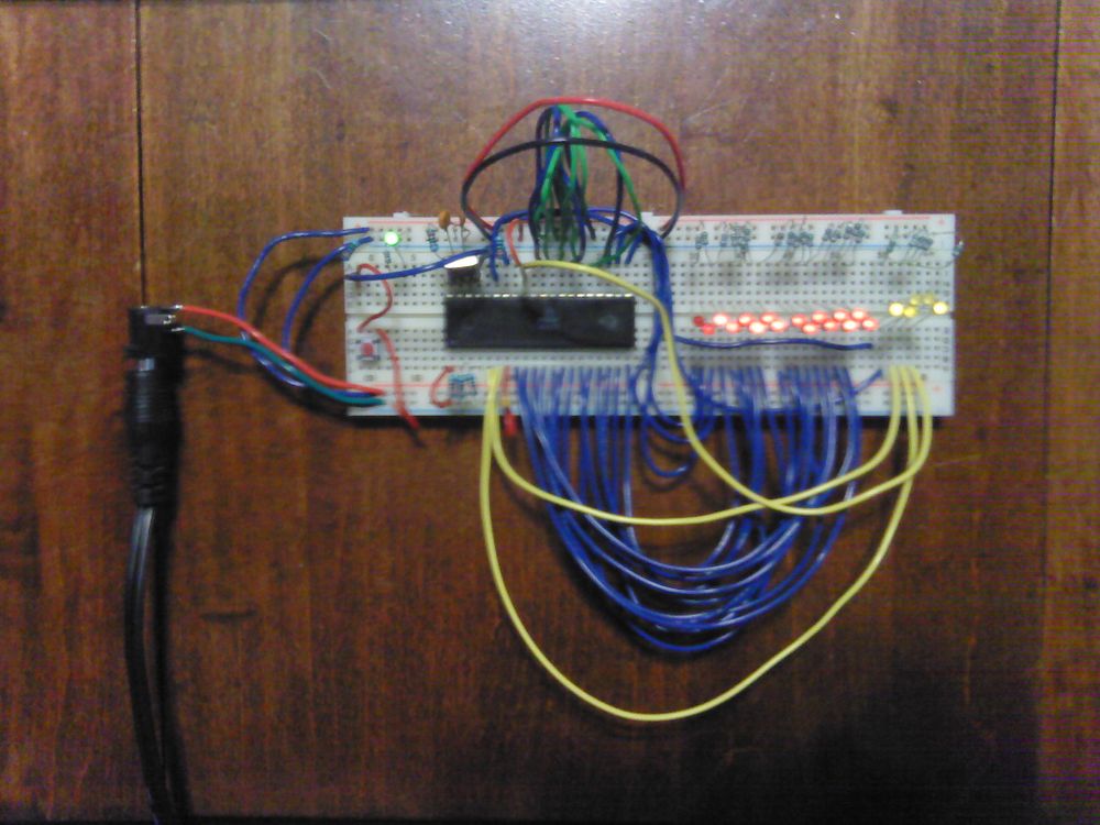
- Here is the schematic in pdf form for you all to follow along in addition to the above pictures as I describe the circuit.
- Primary Schematic for 6809P/6309P Blinkenlights Circuit/CPU Tester Has the RC Circuit as recommended by the MC6809P Datasheet for the RESET pin 37.
- Power Schematic
- Now for the description in its entirety. Of course I started out by inserting an MC6809P (no EP) microprocessor chip into the solderless breadboard leaving a little space for the reset button and power led. I connected the flat side of the Green led to VCC and the other lead to a 1.2K resistor which was connected to GND. Next I inserted a 0.1uf capacitor across VCC and GND as close as possible to pin 7 of the CPU chip.
- Since I had already studied the entire 6809 datasheet very carefully over the past few years, I just went down the left side of the 6809 cpu symbol in the schematic of my Kipper SBC v1 to determine how I wanted to hook up each pin on the chip. The first 2 pins I chose to wire were pins 38 & 39 to which the crystal connects. Each one of the two 27pf capacitors connect to pins 38 & 39. The other lead of each 27pf capacitor connects to ground. I would have used 22pf capacitors as the 6809P datasheet suggests, but the 27pfs were handy.
- I just noticed that the pdfs I have in the dropbox are incorrect. Schematic 1 does not have the RC circuit which my breadboarded circuit is using so I will need to update it. In the meantime, a 2.2K resistor connects Reset pin 37 to VCC. A normally open (NO) pushbutton switch connects Reset pin 37 to ground. A 100uF capacitor is (or will be) connected across the pushbutton switch. I did not have a capacitor of the correct value so I left it off for the time being. Oddly enough, the 6809P cpu boots up every single time I press the reset button. Could the lack of a capacitor in the RESET circuit also be the reason the CPU stops a second or two after pushing the reset button? I'm not sure yet.
- I noticed I have not included the 1.2K resistors I used on the NMI, IRQ, FIRQ, pins 2,3,4 on the schematic. Clearly I need to update the schematic. Halt pin 40 also has a 1.2K resistor connecting Halt to VCC. (Interlude music plays while the schematic is quickly updated.) Ok, now the schematic has been updated to show the simple RC circuit for RESET pin 37. The RC circuit uses a 2.2K resistor. All other resistors are 1K. I used 1.2K resistors instead of 1k resistors as that value was handy and plentiful in my parts bin. I'm thinking of raising this value. Not sure to what yet as I need to see what values I have in my parts bin.
- The data bus is easy as it is hard wired for a $12 - NO-OP opcode. The NO-OP (No Operation) or NOP mnemonic effectively just increments the address bus by one and uses 1 instruction fetch and execute cycle. To wire a NOP to the Data Bus, the Data Bus is tied directly to VCC or GND (Ground) depending on the pin. Out of D0 - D7, D1 pin 30 and D4 pin 27 are tied to VCC. D0 pin 31, D2 pin 29, D3 pin 28, D5 pin 26, D6 pin 25 and D7 pin 24 are tied to GND.
- Now on to the simplest graphic user interface ever created! :) All Address output lines A0 - A15 pins 8 - 23 are connected to a 1.2K resistor which in turn connects to an LED which connects to GND. I connected them to VCC initially and did not realize until later that they should have been connected to GND instead, but since they are all pulsing/blinking in a ripple counter fashion it did not really matter so I never changed them. Ripple Counter Fashion simply means that A0 blinks the fastest, A1 blinks half as fast and so on to A15 which counts the slowest. Instead of using a 4MHZ crystal, I used a 1.8432MHZ crystal laying nearby so I could see a few of the highest bits of the address bus blinking with the naked eye. This is a handy way of making sure the Address Bus is actually pulsing - blinking all the LEDs thus ensuring the CPU is ACTUALLY functioning correctly. Of course you can use an Oscilloscope to make sure. :) Note: When switching an LED from VCC to GND and vice versa, the LED itself has to be reversed.
- An interesting side note is the 6800 CPU actually has an undocumented "Halt and Catch Fire" or HCF op code $9D and $DD that Motorola used during the manufacturing process to check to make sure each 6800 CPU die was functional before they went further on to be cut apart and packaged in the 40 pin DIP style chip. I don't remember if the 6809 has one and I have no info as to whether this simple test feature is found in the 6309 either. Would anyone like to find out if the 6809 or 6309 have any undocumented OP Codes - Mnemonics? :) Inquiring minds want to know!
- I also connected 5 control signals to LEDs. They are the E-Clock pin 34, Q-Clock pin 35, BA pin 6, BS pin 5 and R/!W pin 32. The E & Q clocks show the CPU is generating the clock frequencies. BA and BS with both LEDs off show the CPU is in normal operating mode. The R/!W LED turned on shows the CPU is in read mode. Initially I connected all 5 control signal leds to VCC. The E and Q clock LEDs lit up as did the BA and BS LEDs. The R/!W (Read NOT Write) LED did NOT light up which it should have so I flipped the LED and grounded it instead. Now the R/!W LED lights up correctly. The CPU is only reading from the Data bus and NEVER writes so the R/!W led always stays lit. BA and BS outputs which show the CPU State both should have been low, both leds off, so I switched those leds as well. For correctness, the leds for the the E and Q clocks which pulse at 1/4 of the Master Clock frequency were also switched to GND. The address bus lines were never switched on my breadboard.
- Well, that is about it I think. This circuit is a great why to begin to get familiar with the 6809P and 6309P microprocessors. Starfleet Out! Qaplah! End Transmission! Shalom!


6809/6309 CPU Tester Revisited
April 28, 2016
- As many of you may know, I have been having great difficulty getting my Kipper SBC design running, so I decided to get back to the basics. It's time to make sure I can even get a 6809 CPU running by itself. You say Why? Well, the previous 6809 CPU Tester did run, but only for a short time. I never could get it to stay running. I knew it should run indefinitely, I just didn't know why. This is the story of how I finally got the 6809 CPU Tester running.
- Being frustrated with my Kipper board problems, I decided to research 68000 cpu testers. I figured I needed to see how the big boys did it. I knew the 68000 was a whole different chip altogether, but there had to be some similarities. It turned out there are. You see, when I built the first 6809/6809 cpu tester, I read the datasheet to make sure I did not draw to much current from each address pin for the LED. Or so I thought. I came across a 68000 CPU tester (i.e. Blinkenlights) project that put an inverterr on the address pin between the CPU and the LED. What a simple solution! I didn't think I needed an inverter, but it turns out that I did. I started from scratch once again and built a simpler 6809/6309 CPU tester. I started with the reset circuit. I never really cared for the RC (resistor - capacitor) approach to reset the CPU, so instead I have employed an MC34064P Undervoltage Sensing Circuit in a TO-92 package. Pin 1 connects to the RESET pin of the CPU. Pin 2 connects to VCC and Pin 3 connects to ground. That's it! It is a neat simple solution for my CPU tester. Next was how to create the master clock. I decided to stay with the recommended Motorola design - a crystal and 2 - 22pf capacitors. A Crystal Oscillator in DIP-8 or DIP-16 package can also be used. At this point though, I prefer the crystal and 2 caps solution. Now to take care of all the interrupt inputs, etc. All active low inputs are tied to VCC through a 4.7K resistor for each line. Now for the magic LED indicator to show the CPU is basically working. A 74LS04N inverter is used to buffer the Address line so the CPU does not get blown. The input of the inverter is tied to the A15 address line and the output is tied to the side of the LED with the line or the flat side. The other side to the LED is connected to VCC through a 4.7K resistor. I never can keep straight which end is the cathode and which end is the anode. :)
Undocumented Op Codes
Mnemonics in the Motorola MC6800 CPU
October 8, 2015
- The Following text is quoted from elsewhere on the internet. I searched for "6800 cpu halt and catch fire". One of the links had this to say about the 6800 and I quote"
- The Motorola 6800, MOS Technology 6501, and Zilog z80 (and derivatives) are the three most popular 8 bit microprocessors, one of which were in virtually every personal computer made in the generation BEFORE the IBM PC (c. 1981 and earlier). 8 bit microprocessors have instructions 8 bits wide allowing for 256 possibilities. BUT the Motorola 6800 has 197 valid instructions, leaving 59 so called invalid, illegal or undefined instructions. Programmers must never use an illegal instruction, and if you use an undefined instruction, what happens is not necessarily predictable.
- Halt and Catch fire is in the illegal category on the 6800 and 6502.
- No its maker(s) never called it that (Tech Pundits invented the term HCF)[1] which is a mode where the microprocessor address lines would increment quite fast, and the chip would not try to load a new instruction, so it would repeat forever until power was removed - whatever program WAS running stops if this command is executed.
- Real Fire? Depends on clock speed, cooling, and of course if something sensitive is attached to those rapidly changing address lines. The chip does get hot. But no real evidence of spontaneous combustion!
- Just a smoothly running program that suddenly "Halts and Catches Fire" - it becomes useless.
- Deep Tech (I was just rereading this and I have no idea what this was going to be. Hum)
- Much of what is written below about the Motorola 6800 applies equally to the MOS Technology 6502 - they are similar hardware. In fact Steve Wozniak designed the main board of the Apple I to use the $150 6800, then modified it for the $20 6501 before production began. [2]
- Remember those 59 illegal/undefined/undocumented/invalid instructions on the 6800? Well 6 actually do something that can be (and was in 1977) quantified by Gerry Wheeler of the University of Waterloo.
- (Begin Scholarly Quote) "According to Motorola, there are 197 valid operation codes for the M6800 microprocessor. This means that, of the 256 possible 8-bit combinations, 59 are called invalid instructions.
- ..
- Let me tell you about a couple of the interesting ones. See table 1 for descriptions of six instructions that Motorola didn't tell us about. The mnemonics are, of course, assigned by me.
- ..
- Now for the big surprise. This one has been dubbed HCF for "Halt and Catch Fire". Well, almost.
- When this instruction is run, the only way to see what it is doing is with an oscilloscope. From the user's point of view, the machine halts and defies most attempts to get it restarted. Those persons with indicator lamps on the address bus will see that the processor begins to read all of memory, sequentially, very quickly. In effect, the address bus turns into a 16-bit counter. However, the processor takes no notice of what it is reading....it just reads. The only way out of this race is with the RESET line. The machine ignores the IRQ, NMI, and HALT lines. For all intents and purposes, the processor has halted and caught fire!
- It is quite possible that the HCF instructions are put into the 6800 design intentionally in the interest of production testing of newly fabricated processor chips. This one instruction might provide the automatic test equipment with a quick initial indication of whether the particular processor chip is a total dud, or a prospect for more detailed automatic testing and verification of defect-free operation.
Table 1: A list of six undocumented M6800 instructions and their
definitions.  The operations and operation codes which invoke them
are defined in the column labelled "Result", and the next instruction
address is given in each case.  Halt and Catch Fire (HCF) does not
have a "next instruction" address, because the processor hangs up.
                              Hexadecimal                    Next
Name                Mnemonic  Op Code   Result               Instruction At
------------------  --------  -------   -------------------  --------------
AND accumulators NBA 14 A.B->A PC+1
store ACCA, immed STAA 87 A->PC+2 PC+3
store ACCB, immed STAB C7 B->PC+2 PC+3
store SP, immediate STS 8F SPh->PC+2;SPl->PC+3 PC+4
store IX, immediate STX CF IXh->PC+2;IXl->PC+3 PC+4
Halt and Catch Fire HCF 9D,DD see text N/A
"[3] (end Quote)
Note 1: The column labeled "Next Instruction At" for the HCF instruction(s) is marked "N/A" which means no new instruction is ever loaded so it repeats forever until the power is removed or RESET as previously discussed.
Note 2: There are actually TWO HCF instructions in an M6800, instructions 9D, and DD BOTH cause this leading some digital engineers to suspect partially implemented internal hardware opposed to an intentional test command. Since Motorola intended these to be undocumented, they haven't ever resolved the question to my knowledge.
- "and I end Quote. Interesting indeed! Starfleet Out! Qaplah! End Transmission! Shalom!
Mnemonics in the Motorola MC6809 CPU
June 21, 2016
- This information was found in a text file at the following url.
< http://dragon32.info/info/undocops.html>
- I have made minor updates concerning formatting so the information displays correctly on this wiki page.
#FILE: $RCSfile: undocops.txt $
#DESC: The 'Documented' Undocumented Illegal 6809 Opcodes
#REV: $Revision: 1.1 $
#DATE: $Date: 1995/08/18 14:39:40 $
#AUTHOR: Graham E. Kinns
#DISCLAIMER: All information provided as is etc.
#ARCHIVE: This file is part of the DRGNINFO collection of Dragon info files
#CONTACT: Comments, bugs, revisions, suggestions to Dragon@grempc.demon.co.uk
#HISTORY: 1.0 27/01/94 - Initial results typed up
#RCSID: $Id: undocops.txt 1.1 1995/08/18 14:39:40 Graham Exp $
These results were found by direct experiment on a 6809E in my Dragon using
Mike Kerry's DreamBug monitor on Rom.
All cycles are assumed - I don't have any way of measuring them at present.
Regular Op Codes
Op Mne		Mode	  ~	  #	  Comment
-- ---         ----      -       -         -------
01 NEG		Direct	  6	  2	  Same as op $00 (NEG <$xx)
02 NEG/COM	Direct	  6       2	  If cc.c = 0 then NEG <$xx (op $00)
					  If cc.c = 1 then COM <$xx (op $03)
					  (<$xx) = not(<$xx) + not(cc.c)
05 LSR		Direct	  6	  2	  Same as op $04 (LSR <$xx)
0b DEC	        Direct	  6	  2	  Same as op $0A (DEC <$xx)
14 ??}                                   Seem to be interrupt related
15 ??		}
18 ??
1b ??
38 CWAI	??	  ?	  2	  or something similar.  Doesn't
			                  alter any regs except CC.
3e RESET       Inherent  -	  1	  Forces internal Reset, disables
				          interrupts.
41 NEGA        Inherent  2       1       Same as 40
42 COMA        Inherent  2       1       Same as 43
45 LSRA        Inherent  2       1       Same as 44
4b DECA        Inherent  2       1       Same as 4a
4e CLRA        Inherent  2       1       Same as 4f
51 NEGB        Inherent  2       1       Same as 50
52 COMB        Inherent  2       1       Same as 53
55 LSRB        Inherent  2       1       Same as 54
5b DECB        Inherent  2       1       Same as 5a
5e CLRB        Inherent  2       1       Same as 5f
61 NEG         Indexed   6+      2+      Same as 60 - not tested
62 COM         Indexed   6+      2+      Same as 63 - not tested
65 LSR         Indexed   6+      2+      Same as 64 - not tested
6b DEC         Indexed   6+      2+      Same as 6a - not tested
71 NEG         Extended  7       3       Same as 70 - not tested
72 COM         Extended  7       3       Same as 73 - not tested
75 LSR         Extended  7       3       Same as 74 - not tested
7b DEC         Extended  7       3       Same as 7a - not tested
87 ??
8f ??
c7 ??
cd ??
cf ??
2 Byte Op Code 10
1000 - 100f
1010    [Page switch 2][Page switch 2] - flowchart in data sheet suggests
	 any page switch code after the intial one are ignored
1011    [Page switch 2][Page switch 3] - same as [Page switch 2]
1012 - 101f
1030 - 103e
1040 - 1082
1084 - 108b
108d
108f - 1092
1094 - 109b
109d
10a0 - 10a2
10a4 - 10ab
10ad
10b0 - 10b2
10b4 - 10bb
10bd
10c0 - 10cd
10cf - 10dd
10e0 - 10ed
10f0 - 10ff

2 Byte Op Code 11
1100 - 110f
1110    [Page switch 3][Page switch 2] - same as [Page sw 3]
1111    [Page switch 3][Page switch 3] - same as [Page sw 3]
1112 - 113e
1140 - 1182
1184 - 118b
118d - 1192
1194 - 119b
119d - 11a2
11a4 - 11ab
11ad - 11b2
11b4 - 11bb
11bd - 11ff
In The Beginning
- Let's turn the time machine back to about 2011. I had been looking for work for about three years. One day I decided in addition to that, I would go back and explore my computer roots. Now let's really turn the time machine way back to about 1982.
- In the early 1980s, my first computer was a TRS-80 Color Computer 1. It had 16K of RAM on an F version motherboard that I later upgraded to 64K. I did everything I could to find out information about that little machine. The internet certainly did not exist back then. It fascinated me and held my attention for hours on end. The only printer I had at the time was an ASR-33 Teletype with paper tape reader and punch. I don't remember whether I started out with Color Basic 1.0 or Extended Basic 1.0, but either way my primary storage medium was cassette based only. Boy, that cassette machine was a challenge to work with! :)
- Later on I eventually upgraded to a Color Computer II. The keyboard layout on this machine was the same as before but it was a lot nicer and it came with 64K of RAM! Somewhere along the way I started using 5.25" floppy drives and started experimenting with OS-9 LI v01.00.00 or 01 and for the first time I felt like I could really do something special with this machine.
- Spinning the clock forward a little ways sees me purchasing my first Color Computer 3. Whether the label was TRS-80 or Tandy, I don't remember. All I knew is it had 128K of RAM! Now I really had a great and mighty computer in my collection. Also, at some point in time I eventually installed a Seagate Model Number ST-225 20MB MFM hard drive running OS-9 LII v02.00.01 on a Color Computer 3 with 128K of RAM with a Winchester 8-bit hard drive controller card from Burke and Burke.
- Then the IBM PC revolution began and my computer interests migrated to building an 80286 based PC and I left the Color Computers behind forever, or so I thought.
- I have always wanted to build a 6809 microprocessor based computer of some sort for the express purpose of learning microprocessor interfacing with the best and my favorite microprocessor of all time. I never had the opportunity nor the resources to build a SouthWest Technical Products Company computer back in the late 1970s as I was still in school until my graduation on June 4, 1978. All through school, however, I drooled over all the computer magazines and computer programming books I could find.
- After high school graduation, I went to work with a close friend of mine who used a Motorola Exorciser running an MDOS operating system. It booted up into a monitor program called ExBug. To boot MDOS, the user first entered a one letter command with some sort of parameter and off it went booting MDOS off of an 8" floppy disk drive. Those drives were huge! The system had two drives and an 8-bit MC6800 Microprocessor ran the whole thing.
- Ok, now we are up to about 2011 when I make my decision to build a 6809 microprocessor based computer. I start scouring the internet looking for people who had built any type of 6809 computer or just even had written papers on the subject. Eventually I collected several notebooks full of documentation about several dinky 6809 computer systems.
- Although I had been reading Motorola Data Books for decades, I had actually never built anything. It all always seemed a bit out of my reach. Well, I finally found a very simple 6809 microprocessor based computer that only used 6 chips and you could program it in Basic! Amazingly enough, it turned out it ran a copy of Extended Color Basic from Radio Shack's old Color Computer line that I had used all those years ago. All the graphics routines were removed since the only way to talk to it was to use some type of ASCII CRT terminal or terminal program running on a PC.
The Start of Prototyping 6809 Based Computer Projects
The Little 6802 Computer That Would Never Be Born
- At some point after I graduated from a Cisco course in 2010 I decided to revisit a 6802 based computer project I had started back in my senior year in college that was to be my senior class project. I had been studying on Heathkit's ET-3400 MC6800 Microprocessor training course that year and wanted to build my own little 6800 single board computer. I asked a close friend of mine if he had any thoughts on this subject which he did. He had enough chips laying around to build an MC6802 based computer using an engineering sample of the MC6846 Rom, I/O, & Timer (RIOT) chip which had a little 2KB Monitor called MikBug masked programmed into the rom portion of the chip. The schematic diagram I used to partially wirewrap a prototyping circuit card has since been misplaced or just plain lost, but I had gotten much of the circuit wirewrapped.
- I soon began to realize that I would not have enough time to finish the project before my days at the college would come to a close, so instead of completing that little computer, I built a Transformerless Microphone Preamplifier for my senior project. My buddy made a printed circuit board for it, so I didn't have to wirewrap it. It looked pretty good and actually worked! :) I packed up my little 6802 computer project and put it into storage.
- Now let's move forward through time to the second half of 2010 where we find me looking through all my boxes in storage for my little 6802 computer that had never gotten completed. I searched through box after box looking for that little rascal and began to find various parts of it. I found the prototyping card, a bag of Dual-n-Line (DIP) sockets, and two little plastic boxes of chips in anti-static foam. What I did not find was the schematic for the circuit that had already been partially finished. Finding all these parts and circuit card for the 6802 computer slowly brought my college memories back to the forefront of my mind.
- This was the current state of that project when I found it in my storage boxes that day when I was rummaging through my stuff looking for that little computer. I investigated solderless breadboarding methods on the internet to figure out from whom to buy a solderless breadboard panel to use to attempt to revive this computer project. The panel shown in the section below talking about the SiMon6809 computer is the panel I first started with to build my 6802 based computer.
- Since there was no schematic found with the parts, I began looking on the internet for the schematic I thought I would have used. I figured my buddy probably had gotten the schematic from a Motorola Application Note, so I scoured the internet to try to find such an App. Note. I eventually put together what I thought I would have used for a schematic for this project, but since none of the sockets on the wirewrap card were never labeled, I could not use it as a guide to what I had done. I therefore started building the 6802 again from scratch.
- The antistatic foam was sticking to every single pin of each chip, so I had to take a pocket knife and start scraping all that black foam off of each and every pin on every chip. I can tell you this took quite a while. It had been 31 years since I had first been given those chips! :) I finally settled on a layout on the breadboard for the chips, so I started mounting them one at a time as I finished cleaning the chips. Finally I was done and began wiring up my little computer. I used telephone wire since I had a bunch of it to interconnect the chips.
- I followed the schematic carefully making sure I was always on the correct pin. It took months for me to build this little computer since I had to reread all those chips' datasheets and timing charts all over again. I finally got the whole thing wired up. Figuring everything was correct I starting looking for a power source for the positive five volts required to power this computer.
My Version of Grant Searle's 6-Chip 6809 Computer
- Narrative about my experience designing and building my version of Grant Searle's 6-Chip 6809 Computer. The link to his web site is http://searle.hostei.com/grant/6809/Simple6809.html
- I decided to use Grant's 6-chip 6809 Computer as the basis for my very first 6809 microprocessor based experimental computer. It took me several weeks studying all the datasheets before I felt confident to wire up the 6-chip computer. Initially, I built my 6-chip computer exactly like Grant's, then I added another 8K of RAM using a second 32KB cache RAM chip from an old PC motherboard. When I fired it up for the first time, it passed the smoke time with flying colors, i.e. no smoke! It did not however communicate with my Hyperterminal program I was running on my laptop. I contacted my close friend and mentor and asked him several things about RS-232 communications and he told me that that was one of the hardest parts of a microprocessor circuit to get right. Well, I finally got it to work and I was basically programming in Extended Basic. In fact Grant Searle named his version of Radio Shacks Basic "6809 Extended Basic". I was ecstatic and beside myself with joy! It was Alive! I had done it! I had built my very own 6809 microprocessor based single board computer.
- I didn't take me long before I wanted to add an additional function to my computer. Back to scouring the Internet I go looking for ideas. I finally decided on adding an MC6821 Peripheral Interface Adapter along with an AY-3-8910 Programmable Sound Generator. I wanted to hear my computer. one problem lead to another problem and I finally had to scrap that idea and figure out why my RS-232 port was not working any more. After investigating for awhile, I finally put it down to think. I had been peeking and poking using the Basic interpreter to try to communication with the PIA and the PSG chips, but to no avail. I put my computer down for awhile and fix some more PC desk tops and laptops for some customers for a little while. There weren't that many.
April 9, 2013

- This is my version of Grant Searle's 6-Chip 6809 with some added extras.
- The MC68B09P Microprocessor chip is bottom in left-most column. Above the 6809 is an AS7C256-15PC 8K x 8 bit (32KB) static ram (sram) chip addressed from $0000 to $7FFF.
- Above the sram is a 27128 eprom programmed with Grant Searle's 6809 Extended Basic. The 6809 Extended Basic is basically Radio Shack's (Tandy's) Extended Color Basic with all the graphics commands removed.
- The top chip in the first column is a DM74LS00N Quad 2-Input NAND Gate chip which is used as part of the address decoding logic. This is the only 74LSxx logic chip Grant used in his design.
- In order to add an additional 8KB of sram additional logic is required, so moving over to the second column of chips, the top chip is an SN74LS32N Quad 2-Input Positive OR Gates.
- The second chip is an SW7404N Hex Inverter chip.
- The third chip is a W24257AK-15 8K x 8 bit (32KB) Static Ram chip of which only 8KB is used as the memory map does not allow anymore ram. The extra address lines are grounded.
- The next item down is 7 header pins used to connect to an RS-232 cable.
- The next chip is a MAX232N Dual EIA-232 Drivers and Receivers chip to convert the serial TTL signal levels from/to the MC6850 ACIA chip to RS-232 signal level standards.
- The bottom chip in the second column is an MC6850 Asynchronous Communications Interface Adapter to enable the 6809 to communicate with the outside world via an RS-232 interface cable. The MC6850 chip is addressed at $A000 to $BFFF. The Address decoding logic is incomplete. This is necessary to reduce the chip count in Grant Searle's original design to keep it at just 6 chips total. I thought it was a fantastic design for first time builders to use. My kudos go to Grant Searle for an excellent job well done.
- The first chip in the third column is a 74LS00PC Quad 2-Input NAND gate chip. The three additional logic chips I added to Grants design to enable me to add the additional 8KB of static ram.
- At this point my project was complete with 40KB of Static ram.
- After initially testing my project without the extra 8KB of sram, I wanted to finish filling up the memory map as there was an 8KB hole at $8000 to $9FFF. This hole in the memory map was hollering out to me for more ram, so I added it. It was to be my very first logic circuit design. I designed the logic required to add some static ram at $8000 to $9FFF.
- When I tested my design, it worked correctly the first time. Now I have a total contiguous static ram memory from $0000 to $9FFF.
- The rest of the third column has the logic chips necessary to drive the 32 LEDs so I can see what is happening in real time on the sixteen address bus lines, the eight data bus lines and the eight control lines.
- The second chip in the third column is an SN74LS244N Octal Buffers and Line Drivers with 3-State outputs chip driving eight red LEDs which show the current state of address lines A15 to A8.
- The third chip down is another SN74LS244N Octal Buffers and Line Drivers with 3-State outputs chip driving eight yellow LEDs which show the current state of address lines A7 to A0.
- The fourth chip down on the third column is an SN74LS245N Bi-directional Octal Bus Transceivers with 3-State outputs chip driving eight green LEDs showing the current state of the eight Data bus lines.
- The fifth and last chip in this design has another SN74LS244N Octal Buffers and Line Drivers with 3-State outputs chip driving four green LEDS and four yellow LEDS showing the current state of eight control lines.
- The first pushbutton is the Reset pushbutton used to reset the 6809 microprocessor.
- The second pushbutton is the Halt pushbutton used to halt the 6809 microprocessor.
- I ran into some problems with 6809 microprocessor not powering up correctly. I never saw Buggy's initial message displayed right after the power-on reset cycle of the 6809 microprocessor completed. I installed a halt pushbutton so I could halt the 6809 and hold it in the halted state while I pressed and released the reset pushbutton, then I released the halt pushbutton to bring the 6809 microprocessor from an initial known state which the reset interrupt vector in the monitor program in eprom provides.
July 26th, 2013
- Way back when I initially put together this project and got it running successfully, I started playing around with the addressing of the 68B50 ACIA which implements TTL levels for the RS-232 protocol. Well, something went wrong and communication ceased.
- Well, I have now figured out that I had changed the addressing of the second 32KB RAM chip as well preventing the system to function correctly.
- In addition, since I have been studying all the various Data sheets and seeing how others have implemented logic circuits, I have figured out how to implement 8KB of the 32KB static ram chip with only one logic chip instead of three.
- More study is needed, but I am confident that I will be able to conquer the problem created back in April - May time frame.
My Version of Erturk Kocalar's SiMon6809 Computer
- Narrative about my experience designing and building my version of Erturk Kocalar's SiMon6809. The link to his web site is http://www.8bitforce.com/simon6809/.
- I surf and surf the internet sometimes out of sheer boredom and what do I find, but Erturk Kocalar's SiMon6809 single board computer. I think on this awhile studying the monitor program that runs on it when I see that the monitor program allows the user to enter assembler code straight into memory! No hex bytes to fool with! I loved this. I read on and it even lists the memory back to the user as in an assembler listing! Well, this is just too cool. Wouldn't have all the computer engineers from the 1970s and 1980s loved to have had a monitor like this one and running on my favorite microprocessor too!
- That does it! I have to build this 8-bit 6809 based computer also! Over the next few nights I finally decide on a chip layout on my solderless breadboard and press in all the chips. In one night I end up wiring almost the entire computer. After all it is only 9 chips plus a USB prototype module. My first 6809 computer had 14 chips and 32 LEDs on just about every signal in that computer. I had added the 32 LEDs so I could see if the computer was doing anything. The 6809 microprocessor was functioning just fine. I just could not see anything in HyperTerminal.
- I had to take care of another customer's laptop so I had to put down my SiMon6809 computer for a few days. During this time, I get an offer from a friend, Allen Huffman to host a personal web page on his server. Thank you Allen.
- It is now April 6, 2013, its 11:43 pm and I'm plugging away entering my 6809 single board computer experiments' experiences on a brand new web page! Isn't life great!
- I finally have a picture for my version of Erturk's SiMon6809 computer and here it is.

- My version of Erturk Kocalar's SiMon6809 computer mounted on another solderless breadboard.
- An interesting note about this particular breadboard. I had originally built an MC6802 Microprocessor & MC6846 Rom, I/O & Timer chip based computer with MikBug programmed into the MC6846's rom, but the chips had been sitting in black antistatic foam for so long (since about the 1980-1981 time frame) that it stuck to the pins so badly that even scraping with a fairly good-sized pocket knife blade could not get it all off the pins. I was sadden by the fact that I could not complete this project, so I put it away for awhile thinking I would get back to it some day.
- Well, some day has arrived, but instead of completing my 6802 based computer with a monitor program, I scrapped the entire design put together with telephone wire in favor of a 6809 based computer with a monitor in rom using proper 22 gauge hookup wire instead of the 28 gauge telephone wire. The telephone wire did not stay in the breadboard holes very well anyway.
- Now back to describing this breadboard layout.
- I decided this time to start in the top left corner to mount the MC68B09P microprocessor chip instead of the bottom left corner of the breadboard.
- The second chip is a 27128 16KB eprom programmed with Erturk's monitor program that somehow got called Buggy 1.0. I'd like to hear the story about how the name Buggy came to be. I bet it is an interesting one. There is a long story about the monitor program itself. Erturk actually did not create it. He just modified it to work with the USB FT245R USB chip. In his design, he uses the chip itself, but since I was prototyping my design on breadboard, I needed the chip in a through hole design. I look for a through hole version on FTDI's web site and came across the USB Prototype module which takes the FT245R surface mounted design and puts in onto a little PCB barely the size of a 24 pin chip suitable for breadboarding. Thank you FTDI for this module.
- The third chip in this column is an MT5C1008-35 128KB Static Ram chip configured as 64KB. I'm not yet including any type of Memory Management unit, so I grounded address line A16, thus I have 64KB and not 128KB. Ah, but you say there is not room for the eprom? This is where I start blazing new trails in my young computer electronics designing portion of my life. This is where my design starts to stray from Erturk's Design.
- I am using three SN74LS138N 3-line to 8-line decoder/demultiplexor chips in an address decoding scheme to give me a plethora of addressing choices to put the future additions and features not yet conceived of and yet to be designed for this project.
- The second column first item is a pushbutton for the reset line to reset the 6809 microprocessor.
- The second item is the first of three SN74LS138N 3-line to 8-line decoder/demultiplexor chips to decode the top 4 address lines A15 to A12 to give me eight possible choices. Each output decodes a 4KB area. They are of course, $8xxx, $9xxx, $Axxx, $Bxxx, $Cxxx, $Dxxx, $Exxx, $Fxxx. I pick the $Dxxx output line and feed it into the next SN74LS138N 3-line to 8-line decoder chip.
- The third item is another SN74LS138N 3-line to 8-line decoder/demultiplexor chip configured to further decode address lines A11 to A8 down to again another eight possible choices. With the output of $Dxxx from the previous SN74LS138N chip, the eight possible choices are $D8xx, $D9xx, $DAxx, $DBxx, $DCxx, $DDxx, $DExx, $DFxx. The $DFxx output is fed into the DM74154N 4-line to 16-line decoder chip.
- The fourth item in the second column is the third SN74LS138N 3-line to 8-line decoder/demultiplexor chip to decode address lines A15 to A13 to arrive at yet another eight choices this time to be used for the Eprom chip. These choices are $0000 to $1FFF, $2000 to $3FFF, $4000 to $5FFF, $6000 to $7FFF, $8000 to $9FFF, $A000 to $BFFF, $C000 to $DFFF, and finally $E000 to $FFFF. The $E000 to $FFFF output is feed to the Chip Enable pin of the 27128 16KB Eprom chip. It is also inverted and fed to the chip enable pin of the static ram chip. They way, the eprom or the sram are accessed exclusive of each other. The two are never enabled at the same time.
- The Fifth item is an SN74LS139AN 2-Line to 4-Line decoder/demultiplexor chip to provide the read and write signals to the UM245R USB Prototype module at the proper address.
- The sixth and last item in the second column is a second SN74LS139AN 2-Line to 4-Line decoder/demultiplexor chip to provide the proper read and write signals to the 128KB Static Ram chip and the 27128 16KB Eprom chip.
- The Third column at the very top is a DM74154N 4-Line to 16-line decoder chip to decode the addess lines A7 to A4 to arrive at the third and final stage of the I/O block addressing. The final sixteen choices are $DF0x, $DF1x, $DF2x, $DF3x, $DF4x, $DF5x, $DF6x, $DF7x, $DF8x, $DF9x, $DFAx, $DFBx, $DFCx, $DFDx, $DFEx, and $DFFx. The $DF0x output line is fed to the first SN74LS139AN chip to address the UM245R USB module at $DF00 to $DF0F. I have narrowed a 4KB block of addresses down to sixteen addresses.
- The second chip in the third column is a Dallas DS1287 Real Time Clock chip so my 6809 computer will know what time it is. It is not connected up and won't be until the original design is tested and fully functional. Then I will add this chip into the memory map and start playing with it.
- And last but certainly not least is the UM245R USB Prototyping Module from FTDI and was if I remember correctly about $25. It's a little expensive, but then I did not have to design and build it. This saves me a lot of time. This chip is addressed at $DF00 to $DF0F. I'll have to check the program and documents on the module to be sure, but it takes up only one memory location, so in sixteen bytes I can have, well, 16 USB ports if I so choose. Of course, at this point what would I do with sixteen USB ports. This is a slave USB port, and we would need some master USB ports if I am going to plug up some USB devices to my 6809 computer. I don't know yet how many memory locations one of those modules takes up, so I will leave the rest of these bytes undefined and unimplemented which means the UM245R module will appear sixteen times in the memory map instead of 4096 times or 4K as is in Erturk's original design. Again, Erturk did minimal address decoding to reduce chip count in his SiMon6809 computer to keep it small.
- The USB prototype module in this design is addressed at $DF0x and the FT245R chip in Erturk's original design of SiMon6809 is addressed at $Dxxx. Again this is done to reduce chip count in Erturk's design, but I wanted to further decode the addressing down much further. I wanted to lay the ground work for moving the address decoding for the block of I/O for all communications devices and chips eventually to the $FFxx range. Since you are reading the Cocopedia.com web site, I bet you can guess want I'm leading up to, but for those that are still learning, I won't spoil the surprise yet.
- It's April 9, 2013 and this completes the initial description of my version of Erturk Kocalar's SiMon6809 computer that I've built thus far. I have many plans for this 6809 computer, so stay tuned for further updates to this web page.
- Remember in the beginning I told you I was not able to build an SWTPC 6800 or 6809 computer back in the 1970s and 1980s nor was I able to build an Altair 8800 or IMSAI, and I wanted to experience the thrill of building my own 6809 computer from scratch using proven designs and methods to reduce drastically the trial and errors stage of design. Of course my changes to the original designs will have to be tested. For example, I changed the address location for the USB port. In Erturk's original design, it was located at $D000 in the assembler code for the monitor program. In my project, I set it at $DF00, so I will need to reassemble the monitor program with the new USB port address which is really no problem. I could have left it at $D000 with it replicated 4096 times in the memory map, but I wanted a more versatile design, so I won't be seeing my USB port at $D000, but at #DF00.
- Stay tuned for further updates. :) This is going to get interesting as I get the basics out of the way and start seeing this thing come to life!
My Color Computer Collection
My Coco 3 Setup
April 4, 2013
- Fired up my new Coco 3 for the first time and gazed upon the standard Extended Color Basic copyright message. There it was in living color, my Coco 3 is alive!
April 5, 2013
- After having burnt an eprom with the "HDB-DOS v1.4 DW4 Coco 3" rom image a few weeks back, I install it into my Disto Super Controller. Once I had closed up the super controller, I inserted the cartridge into the Coco 3's cartridge slot and powered up the Coco 3. Behold, my eyes peered on the screen to see the Disk Extended Color Basic copyright message and below it was displayed the HDB-DOS V1.4 DW4 COCO 3 message and the OK prompt appeared with the famous flashing color cycling curser. I did not get any floppy drives out of storage yet, so my test ended here.

April 6, 2013
- The next day saw me looking through all my computer stuff in storage for 3.5" floppy drives. I found a number of them with selectable device select jumpers, so I started a stack of them. I ended up with eight 3.5" drives with changeable drive select jumpers. I took three of them into the house and commenced to connecting up two of the drives.
- I Connected up two 3.5" floppy drives to the Disto Super Controller and formatted a 720KB floppy disk and a 1.44MB floppy disk with the Double-density/High density hole covered up to make the floppy drive think it is a 720KB floppy. Both types of floppies formatted perfectly. I wrote a very simple basic program to read all memory locations from $8000 to $FFFF and display them as characters on the screen. I then saved the program to one of my freshly formatted floppies and typed the command NEW. Now that the basic program is not in memory anymore, I read the program off the floppy and load it into the computer's RAM memory. Then I ran the program and all the bytes stored in the eprom were being displayed as text and graphic characters. It worked perfectly!
April 7, 2013
- I booted VCC on an old Windows XP desktop mini-tower computer with the special fdrawcmd.sys driver installed to enable the system to create coco compatible floppies. I loaded "NitrOS-9 6309 l2 v3.2.9 coco3 80 trk" image into virtual drive 0. I entered the infamous DOS command to boot into NitrOS-9. The white screen appeared and garbage characters filled the screen. I said, "What?". It took me a while to realize my coco 3 is still using an MC68B09EP microprocessor chip. Ah ha! I needed the 6809 boot image. I had been using the 6309 version of the boot image for so long in VCC, that I had completely forgotten that my real coco was still running the original Motorola microprocessor.
April 8, 2013
- I go back to my desktop computer, boot up VCC again this time using the "NitrOS-9 6809 l2 v3.2.9 coco3 80 trk" image in virtual drive 0. I DMODEd drive /d1 changing the cylinders from 35 tracks to 80 tracks with the command "dmode /d1 cyl=50". The cylinder parameter is in hexadecimal - $50 = 80 decimal.
- Then I issue the "format /d1" command, check the floppy disk parameters to make sure they are what I need and answer "Y"(es) to the "Ready" prompt and away it goes formatting a real 3.5" 720KB floppy using a virtual Coco 3. Thanks guys for creating VCC. I love it.
- Once the floppy is formatted, I issue the "backup /d0 /d1" command to backup the NitrOS-9 virtual disk image I booted VCC with to arrive at a real bootable NitrOS-9 floppy disk to use in my real Coco 3.
- Now I go back to my real Coco 3 setup in the living room and I inserted the 6809 version of the NitrOS-9 boot disk into the coco 3's floppy drive, enter the DOS command and behold, NitrOS-9 started booting! :) I love it! My favorite disk operating system is finally booting on my real Coco 3!


- As you can see, the composite video output of the Coco 3 in my setup makes the NitrOS-9 screens almost completely unreadable. Except for the fact that I already know what is on the screen from seeing it in VCC, I would have no idea what is there.
- So I issue a shell command to create a new window hoping I can see little better what the text on the screen actually is with the command "shell i=/W7&".

- Now it is time to test some more 3.5" floppy drives.
- The procedure I use to test a floppy drive is to boot NitrOS-9 and change the cylinders on drive /d1 to $50 and format a floppy disk. If the format is a success, then I backup my boot disk from /d0 to /d1. Then I remove all disks and power cycle the computer. I put the newly made boot disk into drive /d0 and see if NitrOS-9 boots successfully. If the boot finishes with flying colors, I call the floppy drive good.
- Using this procedure, I end up with three good 3.5" floppy drives out of the original eight floppy drives I found with changeable drive select jumpers. During the testing, however, I found a couple of Chinon Model FZ-357 floppy drives with 14 jumper pins giving 9 possible jumper settings that when set to be drive 2 and one at a time are accessed, Drive 0 also is accessed at the same time. They however run fine when set to be drive one. So although I have the cabling to run three 3.5" floppy drives, I effectively can only run two.
- Now here's the kicker. Back in the day I ended up buying several floppy disk controllers. They are, in no particular order, the Disto Super Controller, a Hard Disk Specialist Color Computer Comtroller, a J&M Systems Floppy disk Controller, and the Burke & Burke XT Interface adapter with a Winchester 8-bit ISA card running an MFM 20MB hard drive.
- Now, except for the Hard drive controller for obvious reasons, all the others will drive up to three floppy drives. Well, and this is the interesting part, I was able to get one of them to drive two DSDD 40Trk 5.25" floppy drives and two DSDD 80Trk 5.25" floppy drives. You ask how did I do that? If I remember correctly, in the documentation for the Disto Super Controller, Tony brought out all the signals being controlled correctly somehow making the controller able to support four DSDD drives. I going from 30+ year old memory here, so I'll need to find that documentation to verify this, but I strongly remember this being true. I have an old DEC Dual Full Height 5.25" floppy drive case I had bought from a HAM FEST decades ago with two full height flopyy drives in it that I pulled out and replaced with two 40 track DSDD half height floppy drives and two 80 track DSHD half height floppy drives so I could take advantage of this very feature. At one time in my twenties, I had four half height 5.25" floppy drives running on my Coco 2. Now to figure out how I did it and do it again. There will definitely be more to come on this later.
April 9, 2013

- This is my Coco 3 testing setup in the living room to first get everything going.
April 20, 2013
- As mentioned in the beginning of my Coco 2 Setup section below, I have found out that my Disto Super Controller and my SuperIDE can NOT co-exist together due to address $FF50 being implemented by both controllers. However, since the SuperIDE Interface can hold up to four Disk ROM images in flash, I will eventually be flashing a couple of my favorite Disk rom images to the SuperIDE as soon I can get my Coco 3 MultiPak Interface to work again with my Coco 3 128K machine. Of Course I will be putting the HDB-DOS v1.4 DW4 Coco 3 rom image in the first of the four 16KB banks of flash memory.
- An updated picture of my Coco 3 setup will be forth coming as soon as I make room for a more permanent living space for my Coco 3 computer and all its accessories. :)
April 25, 2013
- Well it's one day before the CoCoFEST and unfortunately I will not make it this year. I understand a number of folks won't be making it for one reason or another. I do have some interesting news about my coco 3 setup though. I have finally conquered the SuperIDE Interface and have setup my Coco 3 in a more permanent living space. I cleaned off one of my computer desks by moving my Cisco networking equipment to a shelf underneath the desktop to make room for my Coco 3. I have setup the Coco 3 with a MultiPak Interface. Slot 3 has the SuperIDE controller with a 256MB Compact Flash Card and a 4GB IDE Hard Drive. The three 3.5" floppy drives I used during my initial testing phase are also connected to a Hard Drive Specialist floppy drive controller which lives in Slot 4.
- I modified the AUTOEXEC.BAS file on virtual drive 0 of the HDB-DOS block to include a command that does something that I can't remember at the moment, but as soon as I get home, I will update this line with the change I made. :) Man, that just slipped my mind!
- The Compact Flash card has a 127MB NitrOS-9 partition and a 256 virtual 35trk SSDD floppy drive HDB-DOS partition. As far as the 4GB HD is concerned, I'm playing with having multiple HDB-DOS partitions. I had a rough start until I realized that the HDB-DOS 1.1D LBA rom image loaded in the flash memory of the SuperIDE controller had a hard drive offset in the image at addresses $D938-$D93A of $052DDC. Evidently the first partition is a NitrOS-9 partition and then an HDB-DOS partition follows after.
- I have employed Robert Gault's AUTOEXEC.BAS listing in his pdf document entitled "Using Large Hard Drives" for navigating the multiple partitions I want. Since this was already put together when I bought it, I needed to modify the AUTOEXEC.BAS file to handle the offset in the rom image. I added a little logic to handle the fact that the logical LSN0 of the first HDB-DOS partition was actually LBA sector 339420, the $052DDC offset mentioned earlier. Once that was completely debugged, and working correctly, it was pretty much smooth sailing from there.
- I checked to make sure that the logic for calculating the current block number was used correctly to set the first LSN of each HDB-DOS partition. Once I was reasonably sure that it could move between different HDB-DOS partition blocks, I formatted the virtual drive 0 on block 1 and saved my customized AUTOEXEC.BAS file. This is actually the second HDB-DOS partition block since the AUTOEXEC.BAS file starts numbering them from zero. I had already formatted all 256 virtual floppy drives of block 0 last night. I then saved another copy on drive 0 of block 0 too. At this point I'm using the standard 35 tracks per disk, 18 sectors per track, single-sided double-density, 256 bytes per sector definition for the 256 virtual floppy drives in those blocks.
- I was able to navigate safely back and forth between partition blocks 0 and 1. Then I moved to block 2, formatted 256 more virtual floppy drives and saved another copy of the AUTOEXEC.BAT file to drive 0 thus giving me 3 defined blocks so far numbered 0, 1 and 2.
- I was pleased to found out that the HDB-DOS DOS command not only looks for a bootable NitrOS-9 floppy disk image in the current drive, but if it does not find one will load and execute the AUTOEXEC.BAS file if any is found. That program is a nice little creation Robert! Thank you for creating it so we all have a template to work from as an example.
- First it displays a title, then my modification which displays the Logical LSN0 for the first partition, then displays how many drives maximum the hard drive will hold for a 4GB drive, and the beginning and ending virtual floppy drive numbers for this block. I plan to add several more options to the program for example one to auto name newly formatted drives with the actual drive number. Another to automatically format a range of drives maybe. That one could be real dangerous as it would not be used very often and would obviously wipe out all data in that block. Maybe I'll just stick to writing that one manually as I need it. There will probably be others as I think of them to make life a little easier handling multiple partition blocks of 256 virtual floppy drives.
- Wow! 768 virtual floppies! I'm not sure at this point if I have that many 5.25" floppies in storage including the 40 trk and 80 trk OS9 formats, the 40 trk ADOS formats, the 80trk CDOS formats and what ever format JDOS used and of course the CHIP BBS 0 rom image too. I didn't just use 35 track floppy disks. As I said before, I always like to adapt things for my own needs. :) I most definitely did a lot of adapting last night. I'm not sure yet how I'm going to handle all those other formats on my hard drive, maybe separate Compact Flash cards. Hum... More thinking to do. How does having 40trk DSDD and 80trk DSDD definitions for the floppy drives in HDB-DOS partition blocks strike you? :)
- Now to scour up some 80trk DSDD 5.25 floppy drives and get them online. I'm not sure if I have any more 40 trk DSDD drives at this point. I wrote down all the model numbers of the 5.25" floppy drives I own and looked them up on the internet. I found out that they all are 1.2MB drives which means that they are 80 trk DSQD (QD for Quad-Density) floppy drives. I need to find at least one 40 trk DSDD floppy drive and at least one blank 5.25" floppy for testing and ultimately read all my old 35trk SSDD floppies and backing them up onto my 768 virtual floppy drives. Whew! Stay tuned.
My Coco 2 Setup
April 20, 2013
- It has been 11 days since I have had time to update my web page. I have found out that there is a shared address $FF50 that both my Disto Super Controller and my SuperIDE Interface implement, much to my dismay, so they can not co-exist together. Therefore I am repurposing my Disto Super Controller for one of my Coco 2 64K computers.
- I have just assembled a Coco 2 version of the HDB-DOS v1.4 DW4 code and burnt the resulting binary file into an AM2764A EPROM and installed it in the first socket of my Disto Super Controller. The second socket has an ADOS eprom in it with two double sided 40 track floppy drives and one double sided 80 track floppy drive defined. The third socket has a CDOS 4.0eprom installed and the fourth socket has a CHIP BBS 0 DOS V1.0 eprom with 80 Track drives defined. As I experiment again with the four DOS eprom images in this Disto Super Controller, I will give further detail on the drive configuration. Hopefully, I will figure out which one can communicate with four floppy drives.
- As of yet, I can not get a fourth physical 3.5" floppy drive to respond on my Coco 3, so this will be an interesting experiment as I relearn what I did all those years ago to get four floppy drives to run on a coco 1, 2, or 3. Hum...
- Initially I will be using a VCR connected to a Composite Video Monitor for my Coco 2 with just the RF output. After I finish my Color Composite Video output board on my first Coco 2 64KB computer, I will switch it out with my original Coco 2 with just the RF output and connect it directly to my color composite video monitor. Then I will keep the VCR in my setup for testing my other Coco 1 and 2 computers as needed.
- A picture of my Coco 2 setup is forth coming as soon as I create a permanent space for it.
April 21, 2013
- As it turns out, the HDB-DOS v1.4 DW4 Coco 2 eprom image I created did not work. I went and got a more recent version of the source files and reassembled HDB-DOS. Like before most but not all loadable binary and rom files were created though the one I needed was created.
- I erased my AM2764A eprom and reburnt the new HDB-DOS v1.4 DW4 Coco 2 rom image file into my AM2764A eprom. I installed the eprom back into my Disto Super Controller and plugged it into my Coco 1 64K computer since it has both Color and Monochrome Composite Video Outputs as well as a mono audio output.
- When I booted the computer I was greeted with the same power-on messages as before, but unlike before I now successfully accessed a Disk Extended Color Basic floppy disk, loaded a Basic program from the floppy and ran it. I was looking at a memory dump of $FF00 - $FFFF! Success!
- I had successfully assembled my own working copy of HDB-DOS v1.4 DW4 Coco2 rom image, burnt it into an eprom, installed the eprom into my favorite floppy disk controller, booted my Coco 1 64KB computer and successfully accessed a 3.5" floppy drive! Of course I will test it with a Coco 1 version of NitrOS-9, but the outlook is good thus far. More exciting things to come. :)
My Combined CoCo 3 & CoCo 1 Computer Data Center!
April 27, 2013

- I now have officially created a permanent home for my Coco 3 and my Coco 1 computers in my newly created Computer Data Center reserved for the Radio Shack & Tandy line of Color Computers. How is that for a long introduction. :)
- On the left side of the picture is a CM-8 Analog RGB Monitor connected to my Coco 3 into which the CoCo 3 compatible MultiPak Interface is plugged into its cartridge port/slot.
- The first slot is empty for now.
- The second slot has a Disto Super Controller installed which is connected to one 5.25" 40 Trk DSDD Floppy drive. The card edge connector on the second floppy drive is positioned differently so it cannot be connected to the floppy drive interface cable at this time.
- The third slot has a SuperIDE Hard Disk Drive Controller installed with a 256MB Compact Flash card in the side slot and a 4GB IDE Hard Disk Drive connected to the IDE compatible connector mounted in the end of the SuperIDE controller.
- In the fourth slot is installed a Hard Drive Specialist Floppy Drive Controller which is connected to three 3.5" Floppy Disk Drives.
- Immediately above the controllers in the MultiPak Interface are the three 3.5" floppy disk drives on the shelf above with the 4GB hard disk drive laying on top of the floppy disk drives. The ATX Power supply is powering all three 3.5" floppy drives and the 4GB hard disk drive.
- On the right side of the computer data center desk is a modified CoCo 1 with a J&M Floppy Disk Drive Controller installed in the cartridge port/slot.
- No floppy drives are connected to this controller at this time due to the fact that all my PC floppy disk drive cables have a little piece of plastic blocking the opening so it cannot be plugged into the J&M controller. The card edge connector in the controller does not have a slot cut into the PCB between contact fingers 3&4 and 5&6. The card edge connector on the PC floppy drive cable does have a piece of plastic in that location of the connecter making connection between the two parts impossible.
- On the shelf above the CoCo 1 is a Radio Shack Dual floppy drive case with two 40 TRK DSDD floppy drives in it. Because the card edge connector is positioned differently in the second floppy drive than the first floppy drive, it cannot be connected to the floppy drive interface cable.
- To the right off the floppy drives is a Color Composite Video Monitor in which is plugged the color composite video output of the CoCo 1. The CoCo 1 you say?!? In a word, Yes! The CoCo 1 has installed a custom Color & Monochrome Composite Video Output Card with a Sound output as well mounted within. Actually it is mounted right on top of the top metal clip top of the shielded RF output unit. The bottom of the PCB is covered with black electrical tape and mounted with a double stick thick foam pad to the top of the RF can.
- Running in the J&M Controller is C-DOS v2.3. In my Disto controller in the third socket is installed an eprom with C-DOS v2.4. I have no documentation for C-DOS, so if one of you out there in the CoCo Community have a copy of the manual for C-DOS and wouldn't mind scanning and emailing me a copy, I would be extremely grateful. Thank you in advance.
- I have modified the Autoexec.bas file in virtual drive 0 of the HDB-DOS partition Block of the compact flash card to include a Menu asking the user to select which set of floppy drives to activate. Answering "1" will activate the set of three 3.5" floppy drives and answering 2 will activate the set of 40 TRK DSDD floppy drives. Just as soon as I find a second 40 TRK DSDD floppy drive with the card edge contacts in the right position so as to be connectable to the floppy drive interface cable, I will be running two drives.

July 26th, 2013
- I was just reviewing my entire web page and realized I didn't finish sharing about the update to the autoexec.bas program on my CoCo 3.
- Below is a picture of the Boot Screen as the Autoexec.bas program now stands.

- In an effort to be fully compatible with ALL of my old CoCo floppies in various formats of which there are many, I have added two 80trk floppy drives to the mix.
- Now my MultiPak Interface for the CoCo 3 is Full!

- Each 5.25" drive's motor turns on and it's LED lights up properly when I try to access the drives one at a time, but they still can not read any CoCo disks. Shoot! I have to go to my old PCs and see if any of those old 5.25" floppy drives still work. I'll let you all know how this challenge gets resolved.
- This is a picture of my 80 track floppy drives.

- And this is my whole setup as it now stands.

- No CoCo 2s in the mix yet. As soon as I populate my Composite Video/Component Video Monitor Driver PCB, I'll be testing one of my CoCo 2s as well. I can hardly wait.
- What I need now is a bunch of RAM in my CoCo 3, a serial cable and off I go into the Wild Blue yonder of Drivewiring! The PC is already setup ready to go and sits on the floor underneath my CoCo Data Center!
- Below the CoCo 1, underneath the desk, on a shelf is my Cisco Network. On the Upper left of the stack is a Printer Spooler with a parallel port that is connected to my Canon Laser Printer.
- To the right of the white printer spooler is a Cisco PIX 506E Firewall Appliance which protects the entire computer network from viruses.
- Underneath both devices is a Cisco 3500XL 48 Port Ethernet Switch with Power On Ethernet capability with Virtual LAN features.
- Below the Cisco switch are two Cisco Content servers with 80GB for storage. Perfect for serving an FTP site on each server. I'd like to put a web site on them if possible.
- Well that about does it for now. If you want further details about anything on this web page just send me an email.
Floppy Drive Woes
October 4, 2013
- Inspiration struck two nights ago and I finally figured out why my 40 track DSDD and 80 track DSHD drives did not work. Well, they were not what I thought they were. Actually they are 1.2MB 80 track DSHD drives! How could I have missed that one! Ugh! I did find two 360K drives in my collection and fully tested them on my Workbench PC and they passed all tests with flying colors! I installed them in my vertical brick and tested them on my CoCo 3 setup in my Data Center and they worked great under HDB-DOS! I can now read all those old 35 track and 40 track SSDD and DSDD floppies in storage. I literally have hundreds, maybe even thousands! That my friends in NOT an exaggeration!
- I also found two 180K 40 Track SSDD drives as well. When I was testing those on my workbench PC, I had not found out what they were yet, so I was stabbing in the dark with the DOS format command parameters. After I returned to the house, while talking with a fellow CoCo buddy on Skype he figured out that they were 180K drives which means they are not 35 track drives as I thought, but 40 track SSDD drives! I had forgotten why flippy floppies were ever born. Duh, to use both sides of the floppies in a single sided drive. Well, I need to go take care of a computer customer, so I'll stop for now. I'll be taking a few more pictures of these two dual drive bricks as well. Take care my friends.
October 24, 2013
- I have now fully tested the two 40 track DSDD 360KB floppy drives on my CoCo 3 as well as the two 40 track SSDD floppy drives. I'm happy to report that all four drives function correctly!
- I had been messing with floppy cables and connectors and managed to mess up my original floppy cable kludge setup, so I ended up ordering a ribbon cable connector crimper so I now I can make all the ribbon cables I need. I made a floppy cable for three 3.5" 1.44MB floppy drives, another floppy cable to fit inside the horizontal brick to connect to the two 40 track SSDD 180KB floppy drives, and a third cable to connect to the two 40 track DSDD 360KB floppy drives. The three 3.5" drives are connected to a floppy controller in Slot 4 of the MPI. The two 360KB drives are connected to a floppy controller in slot 2 and the two 180KB drives are connected to a floppy controller in slot 1.
- Now I can specify which floppy controller and associated floppy drives I wish to use with my basic program menu that boots off the Compact Flash card of the SuperIDE controller in Slot 3 on power up. Remember the one I described earlier? I'm getting sleepy and my eyes are very tired, so I will sign off for now and complete this narrative shortly. Take care my friends and stay turned for more exciting news on this and other activities with my CoCo Data Center!
November 15, 2013
- Though I have not found my 5.25" 720KB floppy drives in storage, I found three reasonably priced ones on ebay, so I can now round out my floppy drive setup with 2 - 5.25" 80 track DSDD 720KB floppy drives in my horizontal brick to replace the two 40 Track SSDD 180KB floppy drives that it currently holds. I will also be creating a 3 floppy drive mix for the express purpose of transferring software from older floppy media to newer floppy media in an effort to preserve the man years of software I have collected and created over the years. This floppy drive setup will consist of 1 - 3.5" 80 track DSDD 1.44MB, 1 - 5.25 40 track DSDD 360KB, & 1 - 5.25" 80 Track DSHD 720KB floppy drives. This way I will be able to transfer old software from the old 5.25" floppy media to newer 3.5" floppy media. As my Drivewire 4 server does not currently run on my desktop computer, I will have to employ an even older HP mini-tower Windows XP computer system to provide the Drivewire 4 File Server needed for my CoCo 3 and CoCo 1. Eventually I plan on creating virtual floppy images of all my old CoCo software, but for the present, I will be picking choice selections of OS-9 disks to backup to 3.5" disks so I can retrieve the drivers I need to operate all my cool Disto cartridges on my CoCo 3 and CoCo 1.
Burning Eproms With My Color Burner
October 3, 2013
- Many years ago when I was much younger I wanted to burn a customized version of ADOS for my CoCo 1. Of course back then in the early to mid 1980's there was no internet to research anything on and the only resources available were books and magazines in local colleges and universities. I scoured all the computer books, magazines and journals I could find in search for an eprom burner which I could use on my CoCo 1. Since that was the only computer I owned back then, I had to look for an EPROM burner interface which run on my CoCo 1 setup.
- At that point in time my CoCo 1 had a Multipak Interface and at least one floppy controller, maybe two. Chronologically speaking though I don't remember what else I might have owned. As I have been collecting CoCo-related parts once again all the memories about the good ole days of learning on and using my CoCos came flooding back to the forefront of my mind. I found something called the Color Burner in a magazine somewhere which was right down my alley! All I do remember is that I built my own interface to burn my own EPROMs for my CoCo 1.
- I was racking my brains trying to remember how I had setup my EPROM burner, but all I could remember was creating some type of custom interface on one of the Color Computer Cartridge Prototype printed circuit boards (PCBs) that Radio Shack use to sell decades ago. That custom card plugged into my Multipak Interface with a ribbon cable connected to that card and running down to another card laying on the table where the EPROM burning actually took place. I also remember having personality modules for different types of EPROM made from 16-pin DIP headers that plugged into a 16-pin IC DIP socket on the Color Burner.
- Recently a discussion started on the CoCo Email List about the Green Mountain Micro Color Burner originally designed by Dennis Bathory-Kitsz who also administers the CoCo Email List. This again sparked my interest in my little Color Burner that I had enjoyed using so many years ago, so I went looking for it again.
- I had ran across it a year or so ago in the midst of looking for something else. You know how it happens that you can usually find everything in the world EXPECT what you are currently looking for. Well, that day I found a whole box of CoCo-related cartridges, disk controllers, etc. including a Burke and Burke MFM Hard Drive Controller which actually used an 8-BIT Winchester MFM Hard Drive Controller Card with an ISA bus from some old IBM PC/XT/AT computer. I seemed to find everything but that Color Burner. I ran across other boxes with more CoCo-related accessories as well. I continued to look everywhere again and again, but I could not remember the spot around my workbench where I had put the Color Burner for safe keeping. Finally I found my Color Burner after remembering I had pulled it out and set it aside so I could possibly use it later on. I was very happy to finally find my wonderful little Color Burner and took some pictures of it so you all can see what I use to burn EPROMs with. :) As it is very late and I'm going bug-eyed trying to see these little words on my laptop, I'm going to have to go to bed for now. I will be posting those pictures very soon. Stay tuned for more exciting adventures with my Cocos!
October 4, 2013
- Well I'm sitting here in my favorite hangout in my "office" in Mickey D's going over my email. I took out my MicroSD memory card from my cell phone expecting to see some pictures of my Color Burner last night. I remember laying out the Color Burner on the table and arranging the cable, but they were not to be found. Hmmmm. This is very strange. I reckon I will have make time to take those pictures and post them here. Take care my friends. :)
Biography
My professional biography will go here.
My Resume
- A link to my resume will go here.
- Professional inquiries may be sent to me using the Contact Information above.
Miscellaneous
- All suggestions for 6809 and 6309 microprocessor based projects and CoCo projects are welcome. Please keep them both positive and helpful.
- Thank you for visiting my little corner of the Wonderful World of the CoCo 1, 2, 3, the 6809 and 6309 microprocessors.
- Starfleet out! End Transmission! Qaplah! Shalom! Keep Having Fun!
--Computerdoc (talk) 21:09, 6 April 2013 (CDT)The Computer Doc
